


Les images sont à titre de référence uniquement. Voir les spécifications du produit
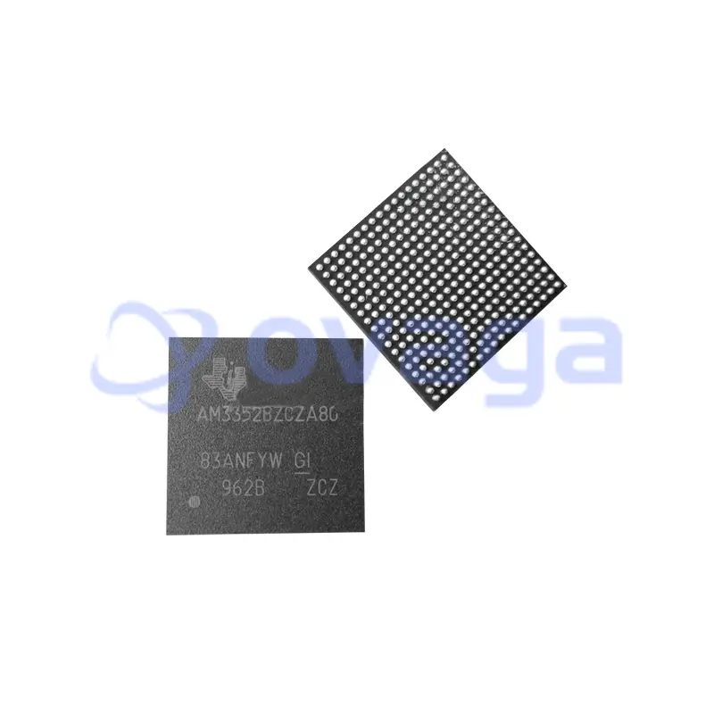
TI AM3358BZCZA80
Microprocessors - MPU Sitara ARM Cortex-A8 MPU


Marques: TI
Pièce Fabricant #: AM3358BZCZA80
Fiche de données: AM3358BZCZA80 Fiche de données (PDF)
Colis/Caisse: LFBGA-324
type de produit: ARM Microcontrollers - MCU
Statut RoHS:
État des stocks: 242 pièces, nouveau original
Warranty: 1 Year Ovaga Warranty - Find Out More
0
1
Ajouter à la nomenclatureAM3358BZCZA80 Description générale
The AM335x microprocessors, based on the ARM Cortex-A8 processor, are enhanced with image, graphics processing, peripherals and industrial interface options such as EtherCAT and PROFIBUS. The devices support high-level operating systems (HLOS). Processor SDK Linux® and TI-RTOS are available free of charge from TI.
The AM335x microprocessor contains the subsystems shown in the Functional Block Diagram and a brief description of each follows:
The contains the subsystems shown in the Functional Block Diagram and a brief description of each follows:
The microprocessor unit (MPU) subsystem is based on the ARM Cortex-A8 processor and the PowerVR SGX™ Graphics Accelerator subsystem provides 3D graphics acceleration to support display and gaming effects.
The PRU-ICSS is separate from the ARM core, allowing independent operation and clocking for greater efficiency and flexibility. The PRU-ICSS enables additional peripheral interfaces and real-time protocols such as EtherCAT, PROFINET, EtherNet/IP, PROFIBUS, Ethernet Powerlink, Sercos, and others. Additionally, the programmable nature of the PRU-ICSS, along with its access to pins, events and all system-on-chip (SoC) resources, provides flexibility in implementing fast, real-time responses, specialized data handling operations, custom peripheral interfaces, and in offloading tasks from the other processor cores of SoC.
Caractéristiques
- Up to 1-GHz Sitara™ ARM® Cortex®-A8 32‑Bit RISC Processor
- NEON™ SIMD Coprocessor
- 32KB of L1 Instruction and 32KB of Data Cache With Single-Error Detection (Parity)
- 256KB of L2 Cache With Error Correcting Code (ECC)
- 176KB of On-Chip Boot ROM
- 64KB of Dedicated RAM
- Emulation and Debug - JTAG
- Interrupt Controller (up to 128 Interrupt Requests)
- On-Chip Memory (Shared L3 RAM)
- 64KB of General-Purpose On-Chip Memory Controller (OCMC) RAM
- Accessible to All Masters
- Supports Retention for Fast Wakeup
- External Memory Interfaces (EMIF)
- mDDR(LPDDR), DDR2, DDR3, DDR3L Controller:
- mDDR: 200-MHz Clock (400-MHz Data Rate)
- DDR2: 266-MHz Clock (532-MHz Data Rate)
- DDR3: 400-MHz Clock (800-MHz Data Rate)
- DDR3L: 400-MHz Clock (800-MHz Data Rate)
- 16-Bit Data Bus
- 1GB of Total Addressable Space
- Supports One x16 or Two x8 Memory Device Configurations
- General-Purpose Memory Controller (GPMC)
- Flexible 8-Bit and 16-Bit Asynchronous Memory Interface With up to Seven Chip Selects (NAND, NOR, Muxed-NOR, SRAM)
- Uses BCH Code to Support 4-, 8-, or 16-Bit ECC
- Uses Hamming Code to Support 1-Bit ECC
- Error Locator Module (ELM)
- Used in Conjunction With the GPMC to Locate Addresses of Data Errors from Syndrome Polynomials Generated Using a BCH Algorithm
- Supports 4-, 8-, and 16-Bit per 512-Byte Block Error Location Based on BCH Algorithms
- mDDR(LPDDR), DDR2, DDR3, DDR3L Controller:
- Programmable Real-Time Unit Subsystem and Industrial Communication Subsystem (PRU-ICSS)
- Supports Protocols such as EtherCAT®, PROFIBUS, PROFINET, EtherNet/IP™, and More
- Two Programmable Real-Time Units (PRUs)
- 32-Bit Load/Store RISC Processor Capable of Running at 200 MHz
- 8KB of Instruction RAM With Single-Error Detection (Parity)
- 8KB of Data RAM With Single-Error Detection (Parity)
- Single-Cycle 32-Bit Multiplier With 64-Bit Accumulator
- Enhanced GPIO Module Provides Shift-In/Out Support and Parallel Latch on External Signal
- 12KB of Shared RAM With Single-Error Detection (Parity)
- Three 120-Byte Register Banks Accessible by Each PRU
- Interrupt Controller (INTC) for Handling System Input Events
- Local Interconnect Bus for Connecting Internal and External Masters to the Resources Inside the PRU-ICSS
- Peripherals Inside the PRU-ICSS:
- One UART Port With Flow Control Pins, Supports up to 12 Mbps
- One Enhanced Capture (eCAP) Module
- Two MII Ethernet Ports that Support Industrial Ethernet, such as EtherCAT
- One MDIO Port
- Power, Reset, and Clock Management (PRCM) Module
- Controls the Entry and Exit of Stand-By and Deep-Sleep Modes
- Responsible for Sleep Sequencing, Power Domain Switch-Off Sequencing, Wake-Up Sequencing, and Power Domain Switch-On Sequencing
- Clocks
- Integrated 15- to 35-MHz High-Frequency Oscillator Used to Generate a Reference Clock for Various System and Peripheral Clocks
- Supports Individual Clock Enable and Disable Control for Subsystems and Peripherals to Facilitate Reduced Power Consumption
- Five ADPLLs to Generate System Clocks (MPU Subsystem, DDR Interface, USB and Peripherals [MMC and SD, UART, SPI, I2C], L3, L4, Ethernet, GFX [SGX530], LCD Pixel Clock)
- Power
- Two Nonswitchable Power Domains (Real-Time Clock [RTC], Wake-Up Logic [WAKEUP])
- Three Switchable Power Domains (MPU Subsystem [MPU], SGX530 [GFX], Peripherals and Infrastructure [PER])
- Implements SmartReflex™ Class 2B for Core Voltage Scaling Based On Die Temperature, Process Variation, and Performance (Adaptive Voltage Scaling [AVS])
- Dynamic Voltage Frequency Scaling (DVFS)
- Real-Time Clock (RTC)
- Real-Time Date (Day-Month-Year-Day of Week) and Time (Hours-Minutes-Seconds) Information
- Internal 32.768-kHz Oscillator, RTC Logic and 1.1-V Internal LDO
- Independent Power-on-Reset (RTC_PWRONRSTn) Input
- Dedicated Input Pin (EXT_WAKEUP) for External Wake Events
- Programmable Alarm Can be Used to Generate Internal Interrupts to the PRCM (for Wakeup) or Cortex-A8 (for Event Notification)
- Programmable Alarm Can be Used With External Output (PMIC_POWER_EN) to Enable the Power Management IC to Restore Non-RTC Power Domains
- Peripherals
- Up to Two USB 2.0 High-Speed DRD (Dual-Role Device) Ports With Integrated PHY
- Up to Two Industrial Gigabit Ethernet MACs (10, 100, 1000 Mbps)
- Integrated Switch
- Each MAC Supports MII, RMII, RGMII, and MDIO Interfaces
- Ethernet MACs and Switch Can Operate Independent of Other Functions
- IEEE 1588v1 Precision Time Protocol (PTP)
- Up to Two Controller-Area Network (CAN) Ports
- Supports CAN Version 2 Parts A and B
- Up to Two Multichannel Audio Serial Ports (McASPs)
- Transmit and Receive Clocks up to 50 MHz
- Up to Four Serial Data Pins per McASP Port With Independent TX and RX Clocks
- Supports Time Division Multiplexing (TDM), Inter-IC Sound (I2S), and Similar Formats
- Supports Digital Audio Interface Transmission (SPDIF, IEC60958-1, and AES-3 Formats)
- FIFO Buffers for Transmit and Receive (256 Bytes)
- Up to Six UARTs
- All UARTs Support IrDA and CIR Modes
- All UARTs Support RTS and CTS Flow Control
- UART1 Supports Full Modem Control
- Up to Two Master and Slave McSPI Serial Interfaces
- Up to Two Chip Selects
- Up to 48 MHz
- Up to Three MMC, SD, SDIO Ports
- 1-, 4- and 8-Bit MMC, SD, SDIO Modes
- MMCSD0 has Dedicated Power Rail for 1.8‑V or 3.3-V Operation
- Up to 48-MHz Data Transfer Rate
- Supports Card Detect and Write Protect
- Complies With MMC4.3, SD, SDIO 2.0 Specifications
- Up to Three I2C Master and Slave Interfaces
- Standard Mode (up to 100 kHz)
- Fast Mode (up to 400 kHz)
- Up to Four Banks of General-Purpose I/O (GPIO) Pins
- 32 GPIO Pins per Bank (Multiplexed With Other Functional Pins)
- GPIO Pins Can be Used as Interrupt Inputs (up to Two Interrupt Inputs per Bank)
- Up to Three External DMA Event Inputs that can Also be Used as Interrupt Inputs
- Eight 32-Bit General-Purpose Timers
- DMTIMER1 is a 1-ms Timer Used for Operating System (OS) Ticks
- DMTIMER4–DMTIMER7 are Pinned Out
- One Watchdog Timer
- SGX530 3D Graphics Engine
- Tile-Based Architecture Delivering up to 20 Million Polygons per Second
- Universal Scalable Shader Engine (USSE) is a Multithreaded Engine Incorporating Pixel and Vertex Shader Functionality
- Advanced Shader Feature Set in Excess of Microsoft VS3.0, PS3.0, and OGL2.0
- Industry Standard API Support of Direct3D Mobile, OGL-ES 1.1 and 2.0, and OpenMax
- Fine-Grained Task Switching, Load Balancing, and Power Management
- Advanced Geometry DMA-Driven Operation for Minimum CPU Interaction
- Programmable High-Quality Image Anti-Aliasing
- Fully Virtualized Memory Addressing for OS Operation in a Unified Memory Architecture
- LCD Controller
- Up to 24-Bit Data Output; 8 Bits per Pixel (RGB)
- Resolution up to 2048 × 2048 (With Maximum 126-MHz Pixel Clock)
- Integrated LCD Interface Display Driver (LIDD) Controller
- Integrated Raster Controller
- Integrated DMA Engine to Pull Data from the External Frame Buffer Without Burdening the Processor via Interrupts or a Firmware Timer
- 512-Word Deep Internal FIFO
- Supported Display Types:
- Character Displays - Uses LIDD Controller to Program these Displays
- Passive Matrix LCD Displays - Uses LCD Raster Display Controller to Provide Timing and Data for Constant Graphics Refresh to a Passive Display
- Active Matrix LCD Displays - Uses External Frame Buffer Space and the Internal DMA Engine to Drive Streaming Data to the Panel
- 12-Bit Successive Approximation Register (SAR) ADC
- 200K Samples per Second
- Input can be Selected from any of the Eight Analog Inputs Multiplexed Through an 8:1 Analog Switch
- Can be Configured to Operate as a 4-Wire, 5-Wire, or 8-Wire Resistive Touch Screen Controller (TSC) Interface
- Up to Three 32-Bit eCAP Modules
- Configurable as Three Capture Inputs or Three Auxiliary PWM Outputs
- Up to Three Enhanced High-Resolution PWM Modules (eHRPWMs)
- Dedicated 16-Bit Time-Base Counter With Time and Frequency Controls
- Configurable as Six Single-Ended, Six Dual-Edge Symmetric, or Three Dual-Edge Asymmetric Outputs
- Up to Three 32-Bit Enhanced Quadrature Encoder Pulse (eQEP) Modules
- Device Identification
- Contains Electrical Fuse Farm (FuseFarm) of Which Some Bits are Factory Programmable
- Production ID
- Device Part Number (Unique JTAG ID)
- Device Revision (Readable by Host ARM)
- Contains Electrical Fuse Farm (FuseFarm) of Which Some Bits are Factory Programmable
- Debug Interface Support
- JTAG and cJTAG for ARM (Cortex-A8 and PRCM), PRU-ICSS Debug
- Supports Device Boundary Scan
- Supports IEEE 1500
- DMA
- On-Chip Enhanced DMA Controller (EDMA) has Three Third-Party Transfer Controllers (TPTCs) and One Third-Party Channel Controller (TPCC), Which Supports up to 64 Programmable Logical Channels and Eight QDMA Channels. EDMA is Used for:
- Transfers to and from On-Chip Memories
- Transfers to and from External Storage (EMIF, GPMC, Slave Peripherals)
- On-Chip Enhanced DMA Controller (EDMA) has Three Third-Party Transfer Controllers (TPTCs) and One Third-Party Channel Controller (TPCC), Which Supports up to 64 Programmable Logical Channels and Eight QDMA Channels. EDMA is Used for:
- Inter-Processor Communication (IPC)
- Integrates Hardware-Based Mailbox for IPC and Spinlock for Process Synchronization Between Cortex-A8, PRCM, and PRU-ICSS
- Mailbox Registers that Generate Interrupts
- Four Initiators (Cortex-A8, PRCM, PRU0, PRU1)
- Spinlock has 128 Software-Assigned Lock Registers
- Mailbox Registers that Generate Interrupts
- Integrates Hardware-Based Mailbox for IPC and Spinlock for Process Synchronization Between Cortex-A8, PRCM, and PRU-ICSS
- Security
- Crypto Hardware Accelerators (AES, SHA, RNG)
- Secure Boot (optional; requires custom part engagement with TI)
- Boot Modes
- Boot Mode is Selected Through Boot Configuration Pins Latched on the Rising Edge of the PWRONRSTn Reset Input Pin
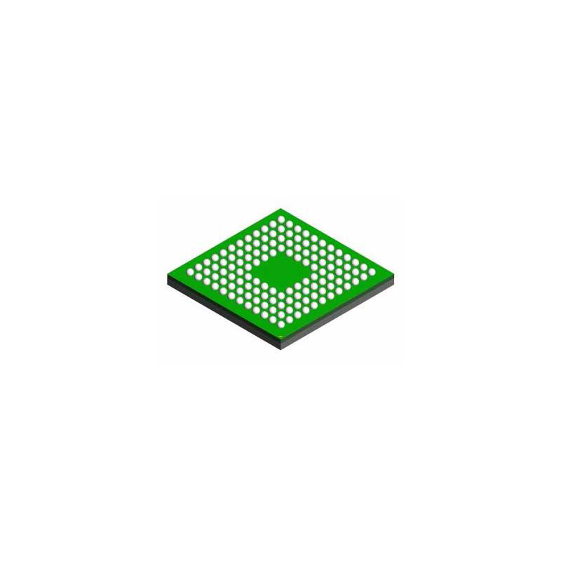
- Packages:
- 298-Pin S-PBGA-N298 Via Channel Package
(ZCE Suffix), 0.65-mm Ball Pitch - 324-Pin S-PBGA-N324 Package
(ZCZ Suffix), 0.80-mm Ball Pitch
- 298-Pin S-PBGA-N298 Via Channel Package
Caractéristiques
| Paramètre | Valeur | Paramètre | Valeur |
|---|---|---|---|
| Arm CPU | 1 Arm Cortex-A8 | Arm (max) (MHz) | 600, 800, 1000 |
| Coprocessors | PRU-ICSS | CPU | 32-bit |
| Graphics acceleration | 1 3D | Display type | 1 LCD |
| Protocols | EtherNet/IP, Ethernet, Profibus, Profinet, Sercos | Ethernet MAC | 2-Port 10/100 PRU EMAC, 2-Port 1Gb switch |
| Hardware accelerators | PRU-ICSS, SGX530 Graphics, Security Accelerator | Features | General purpose, Networking |
| Operating system | Linux, RTOS | Security | Cryptography, Device identity |
| Rating | Catalog | Power supply solution | TPS65216, TPS65218D0 |
| Operating temperature range (°C) | -40 to 105, 0 to 90 |
Expédition
| Type d'expédition | Frais d'expédition | Délai de mise en œuvre | |
|---|---|---|---|
 |
DHL | $20.00-$40.00 (0.50 KG) | 2-5 jours |
 |
FedEx | $20.00-$40.00 (0.50 KG) | 2-5 jours |
 |
UPS | $20.00-$40.00 (0.50 KG) | 2-5 jours |
 |
TNT | $20.00-$40.00 (0.50 KG) | 2-5 jours |
 |
EMS | $20.00-$40.00 (0.50 KG) | 2-5 jours |
 |
LA POSTE AÉRIENNE ENREGISTRÉE | $20.00-$40.00 (0.50 KG) | 2-5 jours |
Délai de traitement : les frais d'expédition dépendent des différentes zones et pays.
Paiement
| Modalités de paiement | Frais de main | |
|---|---|---|
 |
Virement bancaire | facturer des frais bancaires de 30,00 $ US. |
 |
Pay Pal | facturer des frais de service de 4,0 %. |
 |
Carte de crédit | facturez des frais de service de 3,5%. |
 |
Western union | charge US.00 banking fee. |
 |
Paiement de Petit Montant | facturer des frais bancaires de 0,00 $ US. |
Garanties
1. Les composants électroniques que vous achetez incluent une garantie de 365 jours, nous garantissons la qualité du produit.
2. Si certains des articles que vous avez reçus ne sont pas de qualité parfaite, nous organiserons de manière responsable votre remboursement ou votre remplacement. Mais les articles doivent rester dans leur état d’origine.
Emballage
-

Étape1 :Produit
-

Étape2 :Emballage sous vide
-

Étape3 :Sac antistatique
-

Étape4 :Emballage individuel
-

Étape5 :Boîtes d'emballage
-

Étape6 :étiquette d'expédition à code-barres


Tous les produits seront emballés dans un sac antistatique. Expédié avec une protection antistatique ESD.
L'étiquette de l'emballage extérieur ESD utilisera les informations de notre société : numéro de pièce, marque et quantité.
Nous inspecterons toutes les marchandises avant expédition, garantirons que tous les produits sont en bon état et que les pièces sont neuves et correspondent à la fiche technique originale.
Une fois que toutes les marchandises sont garanties sans problème après l'emballage, nous les emballerons en toute sécurité et les enverrons par Global Express. Il présente une excellente résistance à la perforation et à la déchirure ainsi qu’une bonne intégrité du joint.


Points de pièce
-
The AM3358BZCZA80 chip is a high-performance microprocessor from Texas Instruments. It is part of the Sitara™ AM335x family, designed for various embedded applications in industrial automation, home automation, and consumer electronics. The chip features an ARM Cortex-A8 core, running at speeds up to 1GHz, and offers a wide range of peripherals such as USB, Ethernet, CAN, and more.
-
Equivalent
AM3358BZCZA80 is the part number for the AM3358 Sitara processor from Texas Instruments. There are no direct equivalent products to this specific chip, as each chip has its own unique specifications and features. However, there may be other processors in the Sitara family that offer similar functionality, but with different part numbers. -
Features
The AM3358BZCZA80 features a 1GHz ARM Cortex-A8 processor, integrated power-management, and high-performance peripherals such as USB, Ethernet, and LCD controller. It also supports high-performance multimedia interfaces and includes a 3D graphics accelerator, PRU-ICSS for real-time industrial communication, and multiple communication interfaces. -
Pinout
The AM3358BZCZA80 has a pin count of 324 and is a high-performance, low-power System-on-Chip (SoC) processor from Texas Instruments. It is based on the ARM Cortex-A8 core and features various peripherals like UART, SPI, I2C, ADC, Ethernet, and more, making it suitable for applications ranging from industrial automation to portable medical devices. -
Manufacturer
The manufacturer of the AM3358BZCZA80 is Texas Instruments (TI). Texas Instruments is a semiconductor manufacturing company specializing in designing and manufacturing analog and embedded processing chips for various industries including consumer electronics, automotive, industrial, and telecommunications. -
Application Field
The AM3358BZCZA80 is a system-on-chip (SoC) designed by Texas Instruments. It is commonly used in industrial automation, embedded systems, and robotics applications. Its features, such as integrated peripherals, low-power consumption, and real-time processing capabilities, make it suitable for a wide range of applications in industrial control, data acquisition, and communication systems. -
Package
The AM3358BZCZA80 chip is available in a 324-ball BGA (Ball Grid Array) package. Its form factor is rectangular, and the size of the package is typically around 17mm x 17mm.


Nous fournissons des produits de haute qualité, un service attentionné et une garantie après-vente
-

Nous avons des produits riches, pouvons répondre à vos différents besoins.
-

La quantité minimum de commande commence à partir de 1 pièce.
-

Les frais d'expédition internationaux les plus bas commencent à partir de 0,00 $
-

Garantie de qualité de 365 jours pour tous les produits


