Les images sont à titre de référence uniquement. Voir les spécifications du produit
Commandes de plus de
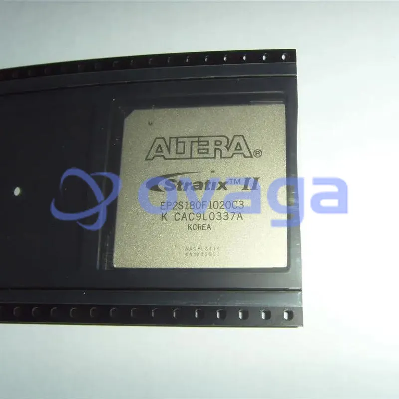
$5000EP2S180F1020C3
With its Field Programmable Gate Array technology, the EP2S180F1020C3 offers customizable solutions for complex designs


Marques: ALTERA CORP
Pièce Fabricant #: EP2S180F1020C3
Fiche de données: EP2S180F1020C3 Fiche de données (PDF)
Colis/Caisse: FBGA-1020
type de produit: FPGAs (Field Programmable Gate Array)
Statut RoHS:
État des stocks: 6 554 pièces, nouveau original
Warranty: 1 Year Ovaga Warranty - Find Out More
0
1
EP2S180F1020C3 Description générale
Boasting a 180,000 logic element capacity and a C3 speed grade, the EP2S180F1020C3 is a formidable Altera Stratix II FPGA designed for high-performance processing. With 1,020 pins and a wide range of I/O options, this FPGA is equipped to handle complex logic functions, high-speed data processing, and real-time signal processing across various industries. Its support for embedded memory blocks, high-speed transceivers, and flexible routing resources ensures that it can meet the demanding requirements of modern applications
Caractéristiques
- The Stratix II family offers the following
- features:
- 15,600 to 179,400 equivalent LEs; see Table 1–1
- New and innovative adaptive logic module (ALM), the basic building block of the Stratix II architecture, maximizes performance and resource usage efficiency
- Up to 9,383,040 RAM bits (1,172,880 bytes) available without reducing logic resources
- TriMatrix memory consisting of three RAM block sizes to implement true dual-port memory and first-in first-out (FIFO) buffers
- High-speed DSP blocks provide dedicated implementation of multipliers (at up to 450 MHz), multiply-accumulate functions, and finite impulse response (FIR) filters
- Up to 16 global clocks with 24 clocking resources per device region
- Clock control blocks support dynamic clock network enable/disable, which allows clock networks to power down to reduce power consumption in user mode
- Up to 12 PLLs (four enhanced PLLs and eight fast PLLs) per device provide spread spectrum, programmable bandwidth, clock switchover, real-time PLL reconfiguration, and advanced multiplication and phase shifting
- Support for numerous single-ended and differential I/O standards
- High-speed differential I/O support with DPA circuitry for 1-Gbps performance
- Support for high-speed networking and communications bus standards including Parallel RapidIO, SPI-4 Phase 2 (POS-PHY Level 4), HyperTransport™ technology, and SFI-4
- Support for high-speed external memory, including DDR and DDR2 SDRAM, RLDRAM II, QDR II SRAM, and SDR SDRAM
- Support for multiple intellectual property megafunctions from Altera MegaCore® functions and Altera Megafunction Partners Program (AMPPSM) megafunctions
- Support for design security using configuration bitstream encryption
- Support for remote configuration updates
Caractéristiques
| Paramètre | Valeur | Paramètre | Valeur |
|---|---|---|---|
| Pbfree Code | No | Rohs Code | No |
| Part Life Cycle Code | Transferred | Ihs Manufacturer | ALTERA CORP |
| Part Package Code | BGA | Package Description | 33 X 33 MM, 1 MM PITCH, FBGA-1020 |
| Pin Count | 1020 | Reach Compliance Code | not_compliant |
| HTS Code | 8542.39.00.01 | Clock Frequency-Max | 717 MHz |
| Combinatorial Delay of a CLB-Max | 4.672 ns | JESD-30 Code | S-PBGA-B1020 |
| JESD-609 Code | e0 | Length | 33 mm |
| Moisture Sensitivity Level | 4 | Number of CLBs | 71760 |
| Number of Inputs | 742 | Number of Logic Cells | 179400 |
| Number of Outputs | 734 | Number of Terminals | 1020 |
| Operating Temperature-Max | 85 °C | Operating Temperature-Min | |
| Organization | 71760 CLBS | Package Body Material | PLASTIC/EPOXY |
| Package Code | BGA | Package Equivalence Code | BGA1020,32X32,40 |
| Package Shape | SQUARE | Package Style | GRID ARRAY |
| Peak Reflow Temperature (Cel) | 220 | Power Supplies | 1.2,1.5/3.3,3.3 V |
| Programmable Logic Type | FIELD PROGRAMMABLE GATE ARRAY | Qualification Status | Not Qualified |
| Seated Height-Max | 3.5 mm | Supply Voltage-Max | 1.25 V |
| Supply Voltage-Min | 1.15 V | Supply Voltage-Nom | 1.2 V |
| Surface Mount | YES | Technology | CMOS |
| Temperature Grade | OTHER | Terminal Finish | TIN LEAD |
| Terminal Form | BALL | Terminal Pitch | 1 mm |
| Terminal Position | BOTTOM | Time@Peak Reflow Temperature-Max (s) | 20 |
| Width | 33 mm |
Expédition
| Type d'expédition | Frais d'expédition | Délai de mise en œuvre | |
|---|---|---|---|
 |
DHL | $20.00-$40.00 (0.50 KG) | 2-5 jours |
 |
FedEx | $20.00-$40.00 (0.50 KG) | 2-5 jours |
 |
UPS | $20.00-$40.00 (0.50 KG) | 2-5 jours |
 |
TNT | $20.00-$40.00 (0.50 KG) | 2-5 jours |
 |
EMS | $20.00-$40.00 (0.50 KG) | 2-5 jours |
 |
LA POSTE AÉRIENNE ENREGISTRÉE | $20.00-$40.00 (0.50 KG) | 2-5 jours |
Délai de traitement : les frais d'expédition dépendent des différentes zones et pays.
Paiement
| Modalités de paiement | Frais de main | |
|---|---|---|
 |
Virement bancaire | facturer des frais bancaires de 30,00 $ US. |
 |
Pay Pal | facturer des frais de service de 4,0 %. |
 |
Carte de crédit | facturez des frais de service de 3,5%. |
 |
Western union | charge US.00 banking fee. |
 |
Paiement de Petit Montant | facturer des frais bancaires de 0,00 $ US. |
Garanties
1. Les composants électroniques que vous achetez incluent une garantie de 365 jours, nous garantissons la qualité du produit.
2. Si certains des articles que vous avez reçus ne sont pas de qualité parfaite, nous organiserons de manière responsable votre remboursement ou votre remplacement. Mais les articles doivent rester dans leur état d’origine.
Emballage
-

Étape1 :Produit
-

Étape2 :Emballage sous vide
-

Étape3 :Sac antistatique
-

Étape4 :Emballage individuel
-

Étape5 :Boîtes d'emballage
-

Étape6 :étiquette d'expédition à code-barres


Tous les produits seront emballés dans un sac antistatique. Expédié avec une protection antistatique ESD.
L'étiquette de l'emballage extérieur ESD utilisera les informations de notre société : numéro de pièce, marque et quantité.
Nous inspecterons toutes les marchandises avant expédition, garantirons que tous les produits sont en bon état et que les pièces sont neuves et correspondent à la fiche technique originale.
Une fois que toutes les marchandises sont garanties sans problème après l'emballage, nous les emballerons en toute sécurité et les enverrons par Global Express. Il présente une excellente résistance à la perforation et à la déchirure ainsi qu’une bonne intégrité du joint.


Points de pièce
-
The EP2S180F1020C3 chip is a field-programmable gate array (FPGA) made by Altera Corporation. It offers high functionality and flexibility for designing and implementing digital circuits. With 180,000 logic elements, 4,040 Kbits of embedded memory, and advanced features like high-speed transceivers, it is suitable for a wide range of applications including telecommunications, industrial automation, and image and signal processing.
-
Equivalent
The equivalent products of EP2S180F1020C3 chip from Altera are Arria II GX FPGAs. -
Features
The EP2S180F1020C3 is a field-programmable gate array (FPGA) manufactured by Altera. It has 180,000 logic elements, 5,808 kilobits of embedded memory, and supports up to 1,280 user I/O pins. It operates at a maximum frequency of 419 MHz and includes built-in transceivers for high-speed data communication. -
Pinout
The EP2S180F1020C3 is an FPGA with 1020 pins. The pins serve various functions such as input/output (I/O), clock inputs, power supply, configuration, and debugging purposes. -
Manufacturer
EP2S180F1020C3 is manufactured by Altera Corporation. Altera is a company that specializes in designing, manufacturing, and selling programmable logic devices. This specific model is a field-programmable gate array (FPGA) manufactured by Altera for use in various electronic applications. -
Application Field
The EP2S180F1020C3 is a field programmable gate array (FPGA) with 180,000 logic elements. It is commonly used in a wide range of applications, including telecommunications, video and image processing, network processing, high-performance computing, industrial control, and automotive electronics. -
Package
The EP2S180F1020C3 chip comes in a Ball Grid Array (BGA) package type. It has a form factor of 1020 pins and a size of 31mm x 31mm.


Nous fournissons des produits de haute qualité, un service attentionné et une garantie après-vente
-

Nous avons des produits riches, pouvons répondre à vos différents besoins.
-

La quantité minimum de commande commence à partir de 1 pièce.
-

Les frais d'expédition internationaux les plus bas commencent à partir de 0,00 $
-

Garantie de qualité de 365 jours pour tous les produits