Les images sont à titre de référence uniquement. Voir les spécifications du produit
Commandes de plus de
$5000LCMXO2-1200HC-6TG100I
Low power consumption with high-speed processing capabilitie


Marques: LATTICE SEMICONDUCTOR CORP
Pièce Fabricant #: LCMXO2-1200HC-6TG100I
Fiche de données: LCMXO2-1200HC-6TG100I Fiche de données (PDF)
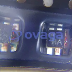
Colis/Caisse: TQFP-100
type de produit: FPGAs (Field Programmable Gate Array)
Statut RoHS:
État des stocks: 6 554 pièces, nouveau original
Warranty: 1 Year Ovaga Warranty - Find Out More
0
1
LCMXO2-1200HC-6TG100I Description générale
The Lattice Semiconductor LCMXO2-1200HC-6TG100I is a versatile and cost-effective FPGA solution designed to meet the demands of modern applications. With 1200 LUTs, 68 I/O pins, 6 macrocells, and 2 PLLs, this FPGA offers a balanced set of resources suitable for a wide range of tasks, from system control to sensor interfacing. Its maximum operating frequency of 100 MHz and 3.3V I/O voltage support make it well-suited for diverse applications, including communication interfaces and industrial control systems. With its low cost and low power consumption, the LCMXO2-1200HC-6TG100I is an attractive option for designers looking to maximize performance while minimizing expenses
Caractéristiques
- Flexible Logic Architecture
- Six devices with 256 to 6864 LUT4s and 19 to 335 I/Os
- Ultra Low Power Devices
- Advanced 65 nm low power process
- As low as 19 µW standby power
- Programmable low swing differential I/Os
- Stand-by mode and other power saving options
- Embedded and Distributed Memory
- Up to 240 Kbits sysMEM™ Embedded Block RAM
- Up to 54 Kbits Distributed RAM
- Dedicated FIFO control logic On-Chip User Flash Memory
- Up to 256 Kbits of User Flash Memory
- 100,000 write cycles
- Accessible through WISHBONE, SPI, I2C and JTAG interfaces
- Can be used as soft processor PROM or as Flash memory
- Pre-Engineered Source Synchronous I/O
- DDR registers in I/O cells
- Dedicated gearing logic
- 7:1 Gearing for Display I/Os
- Generic DDR, DDRX2, DDRX4
- Dedicated DDR/DDR2/LPDDR memory with DQS support
- High Performance, Flexible I/O Buffer
- Programmable sysIO™ buffer supports wide range of interfaces:
- – LVCMOS 3.3/2.5/1.8/1.5/1.2
- – LVTTL
- –PCI
- – LVDS, Bus-LVDS, MLVDS, RSDS, LVPECL
- – SSTL 25/18
- – HSTL 18
- – Schmitt trigger inputs, up to 0.5V hysteresis
- I/Os support hot socketing
- On-chip differential termination
- Programmable pull-up or pull-down mode
Caractéristiques
| Paramètre | Valeur | Paramètre | Valeur |
|---|---|---|---|
| Pbfree Code | Yes | Rohs Code | Yes |
| Part Life Cycle Code | Active | Ihs Manufacturer | LATTICE SEMICONDUCTOR CORP |
| Part Package Code | QFP | Package Description | QFP, QFP100,.63SQ,20 |
| Pin Count | 100 | Reach Compliance Code | compliant |
| ECCN Code | EAR99 | HTS Code | 8542.39.00.01 |
| Samacsys Manufacturer | Lattice Semiconductor | Additional Feature | ALSO OPERATES AT 3.3 V NOMINAL SUPPLY |
| Clock Frequency-Max | 133 MHz | JESD-30 Code | S-PQFP-G100 |
| JESD-609 Code | e3 | Length | 14 mm |
| Moisture Sensitivity Level | 3 | Number of Inputs | 79 |
| Number of Logic Cells | 1280 | Number of Outputs | 79 |
| Number of Terminals | 100 | Operating Temperature-Max | 100 °C |
| Operating Temperature-Min | -40 °C | Package Body Material | PLASTIC/EPOXY |
| Package Code | QFP | Package Equivalence Code | QFP100,.63SQ,20 |
| Package Shape | SQUARE | Package Style | FLATPACK |
| Packing Method | TRAY | Peak Reflow Temperature (Cel) | NOT SPECIFIED |
| Power Supplies | 2.5/3.3 V | Programmable Logic Type | FIELD PROGRAMMABLE GATE ARRAY |
| Qualification Status | Not Qualified | Seated Height-Max | 1.6 mm |
| Supply Voltage-Max | 3.465 V | Supply Voltage-Min | 2.375 V |
| Supply Voltage-Nom | 2.5 V | Surface Mount | YES |
| Terminal Finish | Matte Tin (Sn) | Terminal Form | GULL WING |
| Terminal Pitch | 0.5 mm | Terminal Position | QUAD |
| Time@Peak Reflow Temperature-Max (s) | NOT SPECIFIED |
Expédition
| Type d'expédition | Frais d'expédition | Délai de mise en œuvre | |
|---|---|---|---|
 |
DHL | $20.00-$40.00 (0.50 KG) | 2-5 jours |
 |
FedEx | $20.00-$40.00 (0.50 KG) | 2-5 jours |
 |
UPS | $20.00-$40.00 (0.50 KG) | 2-5 jours |
 |
TNT | $20.00-$40.00 (0.50 KG) | 2-5 jours |
 |
EMS | $20.00-$40.00 (0.50 KG) | 2-5 jours |
 |
LA POSTE AÉRIENNE ENREGISTRÉE | $20.00-$40.00 (0.50 KG) | 2-5 jours |
Délai de traitement : les frais d'expédition dépendent des différentes zones et pays.
Paiement
| Modalités de paiement | Frais de main | |
|---|---|---|
 |
Virement bancaire | facturer des frais bancaires de 30,00 $ US. |
 |
Pay Pal | facturer des frais de service de 4,0 %. |
 |
Carte de crédit | facturez des frais de service de 3,5%. |
 |
Western union | charge US.00 banking fee. |
 |
Paiement de Petit Montant | facturer des frais bancaires de 0,00 $ US. |
Garanties
1. Les composants électroniques que vous achetez incluent une garantie de 365 jours, nous garantissons la qualité du produit.
2. Si certains des articles que vous avez reçus ne sont pas de qualité parfaite, nous organiserons de manière responsable votre remboursement ou votre remplacement. Mais les articles doivent rester dans leur état d’origine.
Emballage
-

Étape1 :Produit
-

Étape2 :Emballage sous vide
-

Étape3 :Sac antistatique
-

Étape4 :Emballage individuel
-

Étape5 :Boîtes d'emballage
-

Étape6 :étiquette d'expédition à code-barres


Tous les produits seront emballés dans un sac antistatique. Expédié avec une protection antistatique ESD.
L'étiquette de l'emballage extérieur ESD utilisera les informations de notre société : numéro de pièce, marque et quantité.
Nous inspecterons toutes les marchandises avant expédition, garantirons que tous les produits sont en bon état et que les pièces sont neuves et correspondent à la fiche technique originale.
Une fois que toutes les marchandises sont garanties sans problème après l'emballage, nous les emballerons en toute sécurité et les enverrons par Global Express. Il présente une excellente résistance à la perforation et à la déchirure ainsi qu’une bonne intégrité du joint.


Points de pièce
-
LCMXO2-1200HC-6TG100I is a low power, versatile FPGA chip from Lattice Semiconductor. It provides cost-effective programmable logic solution for a wide range of applications including consumer electronics, industrial control, communication systems, and more. With 1200 LUTs, 64 Kbits of embedded memory, and low power consumption, it is suitable for various designs that require flexibility and energy efficiency.
-
Equivalent
Some equivalent products of LCMXO2-1200HC-6TG100I chip are LCMXO2-1200HC-6SG32C, LCMXO2-1200HC-6BG256C, and LCMXO2-1200HC-4BG256C. These chips have similar features and performance characteristics, making them suitable replacements for the LCMXO2-1200HC-6TG100I chip in various applications. -
Features
- Lattice MachXO2 FPGA - 1200 LUTs - 6000 system LUT4 equivalents - 128 Kbits embedded memory - 35 I/Os - 6 differentiated I/O standards - Low power consumption - Small form factor (100-pin TQFP package) - Integrated Flash memory - Flexible design options and performance versatility -
Pinout
The LCMXO2-1200HC-6TG100I is a MachXO2 family FPGA with a pin count of 100. It has 1200 LUTs, 8 KB memory, and 61 I/O pins for interface and connectivity applications. This device offers features like I2C and SPI interfaces, PLLs, and embedded memory for design flexibility in low-power, high-volume applications. -
Manufacturer
The manufacturer of the LCMXO2-1200HC-6TG100I is Lattice Semiconductor Corporation. Lattice Semiconductor is an American company that specializes in creating programmable logic devices, software development tools, and IP cores. They focus on providing solutions for the communications, computing, industrial, automotive, and consumer markets. -
Application Field
The LCMXO2-1200HC-6TG100I is commonly used in industrial automation, medical devices, consumer electronics, telecommunications, and automotive applications. It is ideal for applications that require low power consumption, high performance, and high integration such as control systems, data acquisition, communication interfaces, and signal processing. -
Package
The LCMXO2-1200HC-6TG100I chip is in a 100-pin TQFP package with a size of 14mm x 14mm.


Nous fournissons des produits de haute qualité, un service attentionné et une garantie après-vente
-

Nous avons des produits riches, pouvons répondre à vos différents besoins.
-

La quantité minimum de commande commence à partir de 1 pièce.
-

Les frais d'expédition internationaux les plus bas commencent à partir de 0,00 $
-

Garantie de qualité de 365 jours pour tous les produits