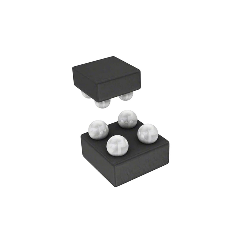
Les images sont à titre de référence uniquement. Voir les spécifications du produit
Commandes de plus de
$5000
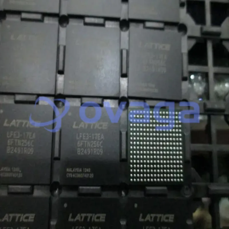
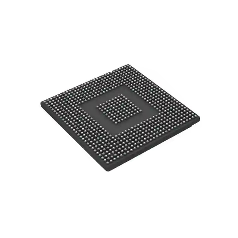
LATTICE LFE3-17EA-6FTN256C

Latticeecp3 ; 17K Luts; 1.2V Rohs Compliant: Yes |Lattice Semiconductor LFE3-17EA-6FTN256C


Marques: Lattice
Pièce Fabricant #: LFE3-17EA-6FTN256C
Fiche de données: LFE3-17EA-6FTN256C Fiche de données (PDF)
Colis/Caisse: FPBGA-256
Statut RoHS:
État des stocks: 9 458 pièces, nouveau original
type de produit: FPGAs (Field Programmable Gate Array)
Warranty: 1 Year Ovaga Warranty - Find Out More
0
1
*Tous les prix sont en USD
| Qté | Prix unitaire | Prix ext |
|---|---|---|
| 1 | $8,664 | $8,664 |
| 10 | $7,634 | $76,340 |
| 30 | $7,008 | $210,240 |
| 100 | $6,481 | $648,100 |
En stock: 9 458 PC
LFE3-17EA-6FTN256C Description générale
Operating at a maximum clock frequency of 550 MHz and with a 1.2V core voltage, the LFE3-17EA-6FTN256C delivers high performance in a compact 256-pin FineLine BGA package. This makes it ideal for applications where space is limited, without compromising on functionality. Additionally, the FPGA includes advanced security features like bitstream encryption and region lockdown, ensuring that your design IP remains protected
Caractéristiques
- Higher Logic Density for Increased System Integration
- 17K to 149K LUTs
- 116 to 586 I/Os
- Embedded SERDES
- 150 Mbps to 3.2 Gbps for Generic 8b10b, 10-bit SERDES, and 8-bit SERDES modes
- Data Rates 230 Mbps to 3.2 Gbps per channel for all other protocols
- Up to 16 channels per device: PCI Express, SONET/SDH, Ethernet (1GbE, SGMII, XAUI), CPRI, SMPTE 3G and Serial RapidIO
- sysDSP™
- Fully cascadable slice architecture
- 12 to 160 slices for high performance multiply and accumulate
- Powerful 54-bit ALU operations
- Time Division Multiplexing MAC Sharing
- Rounding and truncation
- Each slice supports
- — Half 36x36, two 18x18 or four 9x9 multipliers
- — Advanced 18x36 MAC and 18x18 Multiply-Multiply-Accumulate (MMAC) operations
- Flexible Memory Resources
- Up to 6.85Mbits sysMEM™ Embedded Block RAM (EBR)
- 36K to 303K bits distributed RAM
- sysCLOCK Analog PLLs and DLLs
- Two DLLs and up to ten PLLs per device
- Pre-Engineered Source Synchronous I/O
- DDR registers in I/O cells
- Dedicated read/write levelling functionality
- Dedicated gearing logic
- Source synchronous standards support
- — ADC/DAC, 7:1 LVDS, XGMII
- — High Speed ADC/DAC devices
- Dedicated DDR/DDR2/DDR3 memory with DQS support
- Optional Inter-Symbol Interference (ISI) correction on outputs
- Programmable sysI/O™ Buffer Supports Wide Range of Interfaces
- On-chip termination
- Optional equalization filter on inputs
- LVTTL and LVCMOS 33/25/18/15/12
- SSTL 33/25/18/15 I, II
- HSTL15 I and HSTL18 I, II
- PCI and Differential HSTL, SSTL
- LVDS, Bus-LVDS, LVPECL, RSDS, MLVDS
- Flexible Device Configuration
- Dedicated bank for configuration I/Os
- SPI boot flash interface
- Dual-boot images supported
- Slave SPI
- TransFR™ I/O for simple field updates
- Soft Error Detect embedded macro
- System Level Support
- IEEE 1149.1 and IEEE 1532 compliant
- Reveal Logic Analyzer
- ORCAstra FPGA configuration utility
- On-chip oscillator for initialization & general use
- 1.2 V core power supply

Caractéristiques
| Paramètre | Valeur | Paramètre | Valeur |
|---|---|---|---|
| Manufacturer: | Lattice | Product Category: | FPGA - Field Programmable Gate Array |
| RoHS: | Details | Series: | LFE3 |
| Number of Logic Elements: | 17000 LE | Adaptive Logic Modules - ALMs: | 8500 ALM |
| Embedded Memory: | 700 kbit | Number of I/Os: | 133 I/O |
| Supply Voltage - Min: | 1.14 V | Supply Voltage - Max: | 1.26 V |
| Minimum Operating Temperature: | 0 C | Maximum Operating Temperature: | + 85 C |
| Data Rate: | 3.2 Gb/s | Mounting Style: | SMD/SMT |
| Package / Case: | FPBGA-256 | Packaging: | Tray |
| Brand: | Lattice | Distributed RAM: | 36 kbit |
| Embedded Block RAM - EBR: | 700 kbit | Maximum Operating Frequency: | 375 MHz |
| Moisture Sensitive: | Yes | Number of Logic Array Blocks - LABs: | 2125 LAB |
| Operating Supply Current: | 18 mA | Operating Supply Voltage: | 1.2 V |
| Product Type: | FPGA - Field Programmable Gate Array | Factory Pack Quantity: | 90 |
| Subcategory: | Programmable Logic ICs | Total Memory: | 736 kbit |
| Unit Weight: | 0.834123 oz |
Expédition
| Type d'expédition | Frais d'expédition | Délai de mise en œuvre | |
|---|---|---|---|
 |
DHL | $20.00-$40.00 (0.50 KG) | 2-5 jours |
 |
FedEx | $20.00-$40.00 (0.50 KG) | 2-5 jours |
 |
UPS | $20.00-$40.00 (0.50 KG) | 2-5 jours |
 |
TNT | $20.00-$40.00 (0.50 KG) | 2-5 jours |
 |
EMS | $20.00-$40.00 (0.50 KG) | 2-5 jours |
 |
LA POSTE AÉRIENNE ENREGISTRÉE | $20.00-$40.00 (0.50 KG) | 2-5 jours |
Délai de traitement : les frais d'expédition dépendent des différentes zones et pays.
Paiement
| Modalités de paiement | Frais de main | |
|---|---|---|
 |
Virement bancaire | facturer des frais bancaires de 30,00 $ US. |
 |
Pay Pal | facturer des frais de service de 4,0 %. |
 |
Carte de crédit | facturez des frais de service de 3,5%. |
 |
Western union | charge US.00 banking fee. |
 |
Paiement de Petit Montant | facturer des frais bancaires de 0,00 $ US. |
Garanties
1. Les composants électroniques que vous achetez incluent une garantie de 365 jours, nous garantissons la qualité du produit.
2. Si certains des articles que vous avez reçus ne sont pas de qualité parfaite, nous organiserons de manière responsable votre remboursement ou votre remplacement. Mais les articles doivent rester dans leur état d’origine.
Emballage
-

Étape1 :Produit
-

Étape2 :Emballage sous vide
-

Étape3 :Sac antistatique
-

Étape4 :Emballage individuel
-

Étape5 :Boîtes d'emballage
-

Étape6 :étiquette d'expédition à code-barres


Tous les produits seront emballés dans un sac antistatique. Expédié avec une protection antistatique ESD.
L'étiquette de l'emballage extérieur ESD utilisera les informations de notre société : numéro de pièce, marque et quantité.
Nous inspecterons toutes les marchandises avant expédition, garantirons que tous les produits sont en bon état et que les pièces sont neuves et correspondent à la fiche technique originale.
Une fois que toutes les marchandises sont garanties sans problème après l'emballage, nous les emballerons en toute sécurité et les enverrons par Global Express. Il présente une excellente résistance à la perforation et à la déchirure ainsi qu’une bonne intégrité du joint.


Points de pièce
-
The LFE3-17EA-6FTN256C chip is a field-programmable gate array (FPGA) produced by Lattice Semiconductor. It features a 17K LUT (Look-Up Table) architecture and uses a 40 nm process technology. This high-performance chip offers low power consumption, excellent system integration, and is suitable for a wide range of applications in industries such as communications, automotive, and industrial automation.
-
Equivalent
The equivalent products of LFE3-17EA-6FTN256C chip include LFE3-17EA-6FN484C, LFE3-17EA-6FTG256C, and LFE3-17EA-6LN256C. -
Features
The LFE3-17EA-6FTN256C is a low-power, field-programmable gate array (FPGA) by Lattice Semiconductor. It offers 17,076 Look-Up Tables (LUTs), 58.8Kb Distributed Memory, 3.5Kb RAM, 64-bit DDR3 memory interface, and 256-ball fine pitch BGA package. It supports up to 293 input/outputs (IOs) with various additional features for efficient design implementation. -
Pinout
The LFE3-17EA-6FTN256C is an FPGA (Field-Programmable Gate Array) with a pin count of 256. It is part of the Lattice ECP3 family and offers a range of general-purpose I/O (Input/Output) functions. -
Manufacturer
The manufacturer of the LFE3-17EA-6FTN256C is Lattice Semiconductor Corporation. It is a semiconductor company that specializes in programmable logic devices, such as field-programmable gate arrays (FPGAs), and related software development tools. -
Application Field
The application areas of the LFE3-17EA-6FTN256C include communication systems, video and image processing, industrial automation, automotive systems, and medical equipment. It is a low-power FPGA with high processing capability, making it suitable for a wide range of applications that require high-performance and low-power consumption. -
Package
The LFE3-17EA-6FTN256C chip comes in a FBGA (Fine-pitch Ball Grid Array) package type. Its form factor is 17 x 17 mm, and it has a size of 289 square millimeters.


Nous fournissons des produits de haute qualité, un service attentionné et une garantie après-vente
-

Nous avons des produits riches, pouvons répondre à vos différents besoins.
-

La quantité minimum de commande commence à partir de 1 pièce.
-

Les frais d'expédition internationaux les plus bas commencent à partir de 0,00 $
-

Garantie de qualité de 365 jours pour tous les produits