

Les images sont à titre de référence uniquement. Voir les spécifications du produit
ON NB3V1104CDTR2G

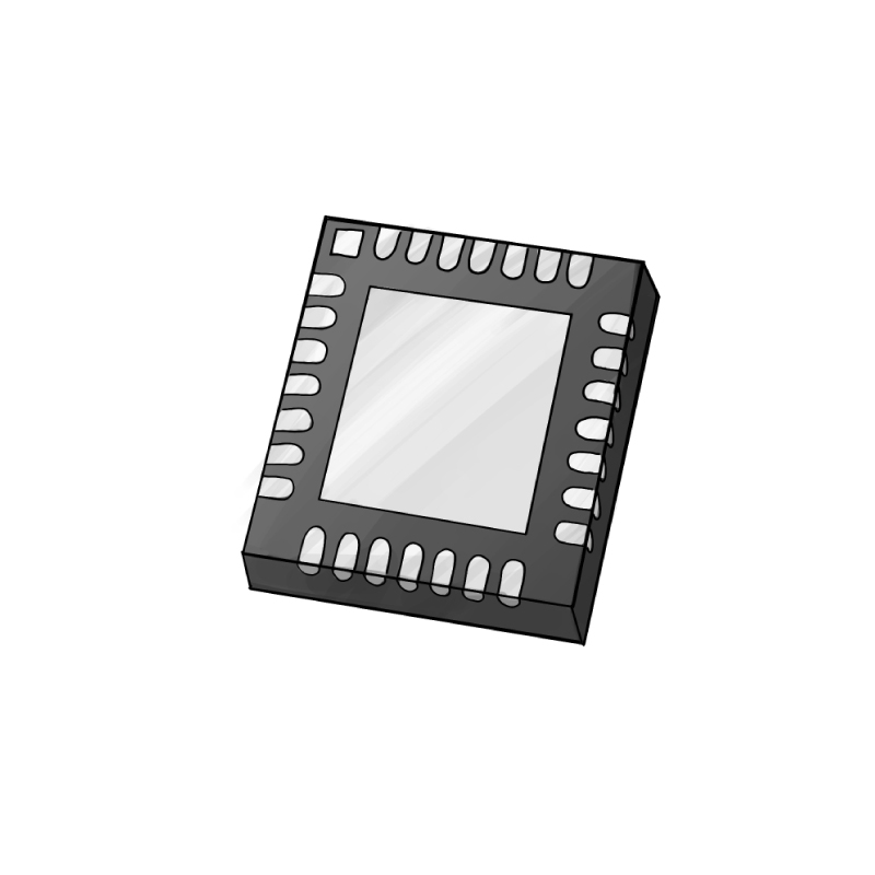
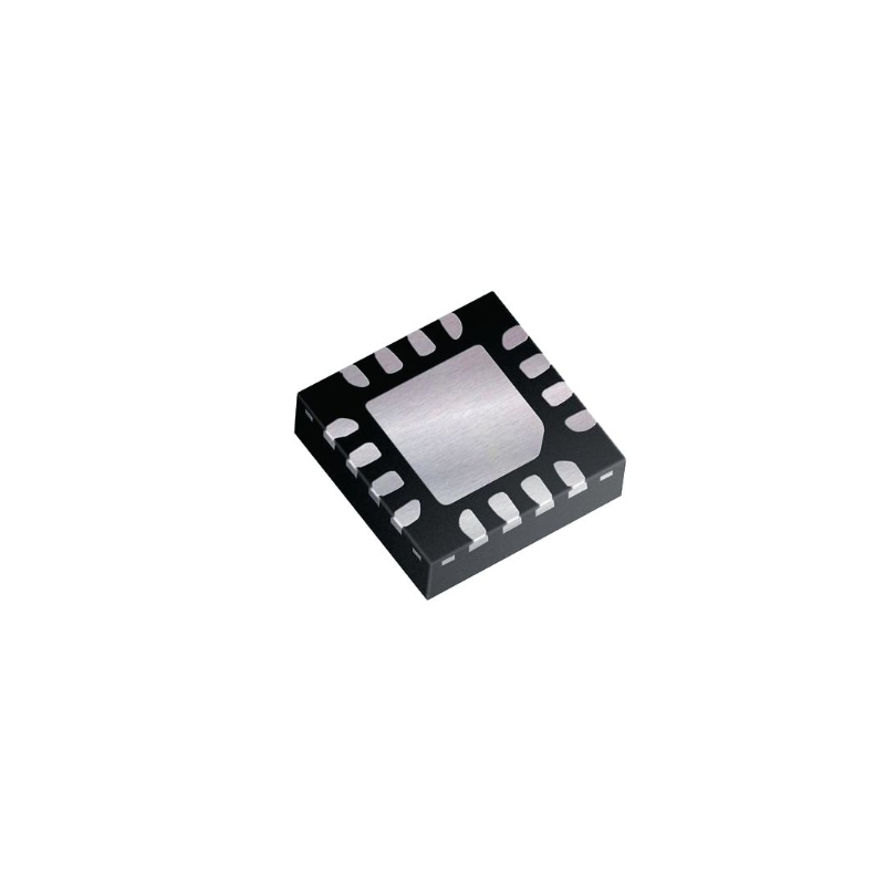
Clock Fanout Buffer (Distribution) IC 1:4 250 MHz 8-TSSOP (0.173", 4.40mm Width)


Marques: ON Semiconductor, LLC
Pièce Fabricant #: NB3V1104CDTR2G
Fiche de données: NB3V1104CDTR2G Datasheet (PDF)
Colis/Caisse: TSSOP-8
Statut RoHS:
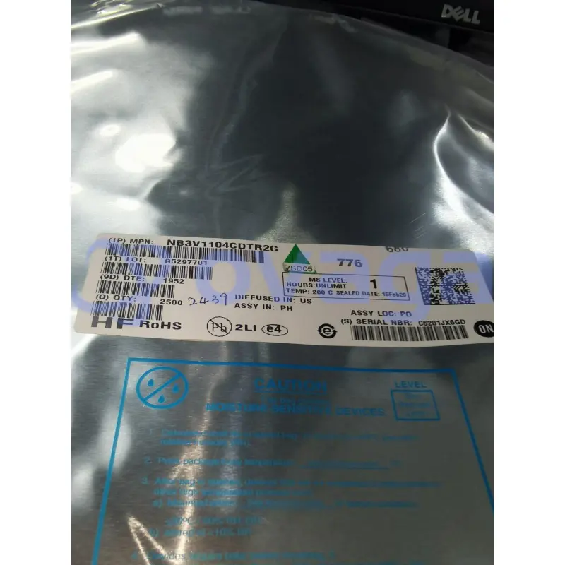
État des stocks: 2167 pièces, nouveau original
type de produit: CI d'horloge et de minuterie
Warranty: 1 Year Ovaga Warranty - Find Out More
0
1
*Tous les prix sont en USD
| Qté | Prix unitaire | Prix ext |
|---|---|---|
| 1 | $2,267 | $2,267 |
| 10 | $1,960 | $19,600 |
| 30 | $1,768 | $53,040 |
| 100 | $1,572 | $157,200 |
| 500 | $1,483 | $741,500 |
| 1000 | $1,444 | $1444,000 |
In Stock:2167 PCS
NB3V1104CDTR2G Description générale
The NB3V1104C is a member of the NB3V110xC a modular, high−performance, low−skew, general purpose LVCMOS clock buffer family. The device has a 1:4 fan-out. The family of devices is designed with a modular approach. Different fan-out variations, 1:2, 1:3, 1:4, 1:6 and 1:8, are available. All of the devices are pin compatible to each other for easy handling. All family members share the same high performing characteristics like low additive jitter, low skew, and wide operating temperature range. The NB3V110xCsupports an asynchronous output enable control (OE) which switchesthe outputs into a low state when OE is low. The NB3V110xC operatein a 3.3 V, 2.5 V and 1.8 V environment and are characterized for operation from –40°C to 105°C.
Caractéristiques
- High−Performance 1:4 LVCMOS Clock Buffer
- Very Low Output−to−Output Skew < 50 ps
- Supply Voltage: 3.3 V, 2.5 V or 1.8 V
- Available in 8−Pin TSSOP
- Operating Temperature Range: –40°C to 105°C
- Low Additive Jitter
- fmax = 250 MHz for 3.3 V; fmax = 180 MHz for 2.5 V; fmax = 133 MHz for 1.8 V
- These Devices are Pb−Free and are RoHS Compliant
Application
- Clock Distribution
- Networking and Data Communication
- High-end Computing
Caractéristiques
| Paramètre | Valeur | Paramètre | Valeur |
|---|---|---|---|
| Manufacturer: | ON Semiconductor | Product Category: | Clock Buffer |
| RoHS: | Y | Series: | NB3V110xC |
| Packaging: | Reel | Brand: | ON Semiconductor |
| Product Type: | Clock Buffer | Factory Pack Quantity: | 2500 |
| Subcategory: | Clock & Timer ICs | Tags | NB3V1, NB3V, NB3 |
| Source Content uid | NB3V1104CDTR2G | Pbfree Code | Yes |
| Part Life Cycle Code | Active | Ihs Manufacturer | ONSEMI |
| Package Description | TSSOP-14 | Manufacturer Package Code | 948S-01 |
| Reach Compliance Code | compliant | HTS Code | 8542.39.00.01 |
| Factory Lead Time | 71 Weeks | Samacsys Manufacturer | onsemi |
| Additional Feature | ALSO OPERATES AT 2.5V AND 3.3V VCC NOMINAL SUPPLY | Family | NB3V |
| Input Conditioning | STANDARD | JESD-30 Code | R-PDSO-G14 |
| Logic IC Type | LOW SKEW CLOCK DRIVER | Moisture Sensitivity Level | 1 |
| Number of Functions | 1 | Number of Inverted Outputs | |
| Number of Terminals | 14 | Number of True Outputs | 4 |
| Output Characteristics | 3-STATE | Package Body Material | PLASTIC/EPOXY |
| Package Code | TSSOP | Package Shape | RECTANGULAR |
| Package Style | SMALL OUTLINE, THIN PROFILE, SHRINK PITCH | Packing Method | TR |
| Peak Reflow Temperature (Cel) | 260 | Surface Mount | YES |
| Temperature Grade | INDUSTRIAL | Terminal Finish | NICKEL PALLADIUM GOLD |
| Terminal Form | GULL WING | Terminal Position | DUAL |
| Time@Peak Reflow Temperature-Max (s) | 30 |
Expédition
| Type d'expédition | Frais d'expédition | Délai de mise en œuvre | |
|---|---|---|---|
 |
DHL | $20.00-$40.00 (0.50 KG) | 2-5 jours |
 |
FedEx | $20.00-$40.00 (0.50 KG) | 2-5 jours |
 |
UPS | $20.00-$40.00 (0.50 KG) | 2-5 jours |
 |
TNT | $20.00-$40.00 (0.50 KG) | 2-5 jours |
 |
EMS | $20.00-$40.00 (0.50 KG) | 2-5 jours |
 |
LA POSTE AÉRIENNE ENREGISTRÉE | $20.00-$40.00 (0.50 KG) | 2-5 jours |
Délai de traitement : les frais d'expédition dépendent des différentes zones et pays.
Paiement
| Modalités de paiement | Frais de main | |
|---|---|---|
 |
Virement bancaire | facturer des frais bancaires de 30,00 $ US. |
 |
Pay Pal | facturer des frais de service de 4,0 %. |
 |
Carte de crédit | facturez des frais de service de 3,5%. |
 |
Western union | charge US.00 banking fee. |
 |
Paiement de Petit Montant | facturer des frais bancaires de 0,00 $ US. |
Garanties
1. Les composants électroniques que vous achetez incluent une garantie de 365 jours, nous garantissons la qualité du produit.
2. Si certains des articles que vous avez reçus ne sont pas de qualité parfaite, nous organiserons de manière responsable votre remboursement ou votre remplacement. Mais les articles doivent rester dans leur état d’origine.
Emballage
-

Étape1 :Produit
-

Étape2 :Emballage sous vide
-

Étape3 :Sac antistatique
-

Étape4 :Emballage individuel
-

Étape5 :Boîtes d'emballage
-

Étape6 :étiquette d'expédition à code-barres


Tous les produits seront emballés dans un sac antistatique. Expédié avec une protection antistatique ESD.
L'étiquette de l'emballage extérieur ESD utilisera les informations de notre société : numéro de pièce, marque et quantité.
Nous inspecterons toutes les marchandises avant expédition, garantirons que tous les produits sont en bon état et que les pièces sont neuves et correspondent à la fiche technique originale.
Une fois que toutes les marchandises sont garanties sans problème après l'emballage, nous les emballerons en toute sécurité et les enverrons par Global Express. Il présente une excellente résistance à la perforation et à la déchirure ainsi qu’une bonne intégrité du joint.


Points de pièce
-
The NB3V1104CDTR2G chip is a voltage controlled oscillator (VCO) designed for low phase noise applications. It operates at a frequency range of 150MHz to 190MHz and provides an output in the form of a square wave. This chip is commonly used in communication systems, radio frequency (RF) equipment, and wireless devices to generate stable and accurate clock signals.
-
Features
Features of NB3V1104CDTR2G include a low power consumption of 3 µA, a wide voltage supply range of 1.65V to 5.5V, a compact size of 1.2 x 1.2 mm, a wide temperature range of -40°C to +85°C, and a stable operation with low jitter. It also offers a 2.5V compatibility and supports I2C interface. -
Pinout
The NB3V1104CDTR2G is a 1:4 clock buffer with a pin count of 16. Its functions include voltage level translation, clock distribution, and clock signal buffering for various applications. -
Manufacturer
The manufacturer of the NB3V1104CDTR2G is ON Semiconductor. ON Semiconductor is a multinational semiconductor manufacturing company that specializes in a wide range of products, including power management, signal conditioning, custom devices, and standard components. They provide innovative solutions for various industries, including automotive, industrial, communication, and consumer electronics. -
Application Field
The NB3V1104CDTR2G is a high-speed clock and data recovery IC designed for applications that require data transfer over long distances. It is commonly used in optical communication systems, fiber-optic networks, and high-speed data transmission applications in telecommunications and networking. -
Package
The NB3V1104CDTR2G chip is available in a package type called DFN-6 (Dual Flat No-Lead). It has a form factor of 3mm x 3mm and a size of approximately 15.4mm².

Fiche de données PDF
Nous fournissons des produits de haute qualité, un service attentionné et une garantie après-vente
-

Nous avons des produits riches, pouvons répondre à vos différents besoins.
-

La quantité minimum de commande commence à partir de 1 pièce.
-

Les frais d'expédition internationaux les plus bas commencent à partir de 0,00 $
-

Garantie de qualité de 365 jours pour tous les produits


Notes et avis
Ovaga's website is easy to use and their selection of electronic components is unparalleled.


Average products, but quick shipping.