Les images sont à titre de référence uniquement. Voir les spécifications du produit
Commandes de plus de
$5000ADI ADL5201ACPZ-R7
Reliable RF amplifier solution with Hz bandwidth and compact EP T/R package


Marques: Analog Devices Inc.
Pièce Fabricant #: ADL5201ACPZ-R7
Fiche de données: ADL5201ACPZ-R7 Datasheet (PDF)
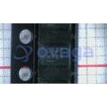
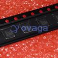
Colis/Caisse: LFCSP-24
Statut RoHS:
État des stocks: 2 769 pièces, nouveau original
Warranty: 1 Year Ovaga Warranty - Find Out More
0
1
ADL5201ACPZ-R7 Description générale
The ADL5201 is a digitally controlled, variable gain, wide band-width amplifier that provides precise gain control, high IP3, and low noise figure. The excellent distortion performance and high signal bandwidth make the ADL5201 an excellent gain control device for a variety of receiver applications. The ADL5201 also incorporates a low power mode option that lowers the supply current.
For wide input dynamic range applications, the ADL5201 provides a broad 31.5 dB gain range with 0.5 dB resolution. The gain is adjustable through multiple gain control interface options: parallel, serial peripheral interface, and up/down.
Incorporating proprietary distortion cancellation techniques, the ADL5201 achieves an output IP3 of greater than 47 dBm at frequencies approaching 200 MHz for most gain settings.
The ADL5201 is powered on by applying the appropriate logic level to the PWUP pin. The quiescent current of the ADL5201 is typically 80 mA in low power mode. When configured in high performance mode for more demanding applications, the quiescent current is 110 mA. When powered down, the ADL5201 consumes less than 7 mA and offers excellent input-to-output isolation. The gain setting is preserved during power-down.
Fabricated on an Analog Devices, Inc., high speed SiGe process, the ADL5201 provides precise gain adjustment capabilities with good distortion performance and low phase error. The ADL5201 amplifier comes in a compact, thermally enhanced, 24-lead, 4 mm × 4 mm LFCSP package and operates over the temperature range of −40°C to +85°C.
Caractéristiques
- 0.5 dB ± 0.1 dB step size
- 150 Ω differential input and output
- 7.5 dB noise figure at maximum gain
- OIP3 > 50 dBm at 200 MHz
- Wide input dynamic range
- Multiple control interface options Parallel 6-bit control interface (with latch) Serial peripheral interface (SPI) (with fast attack) Gain up/down mode
- Low power mode option
- Power-down control
- Single 5 V supply operation
- 24-lead LFCSP 4 mm x 4 mm package
Application
- Differential ADC drivers
- High IF sampling receivers
- High output power IF amplification
- Instrumentation
Caractéristiques
| Paramètre | Valeur | Paramètre | Valeur |
|---|---|---|---|
| Product Category | RF Amplifier | RoHS | Details |
| Package / Case | LFCSP-24 | Type | Variable Gain Amplifiers |
| Technology | Si | Operating Frequency | 700 MHz |
| Gain | 20 dB | Operating Supply Voltage | 4.5 V to 5.5 V |
| NF - Noise Figure | 7.5 dB | OIP3 - Third Order Intercept | 50 dBm |
| Operating Supply Current | 110 mA | Minimum Operating Temperature | - 40 C |
| Maximum Operating Temperature | + 85 C | Series | ADL5201 |
| Brand | Analog Devices | Development Kit | ADL5201-EVALZ |
| Moisture Sensitive | Yes | Number of Channels | 1 Channel |
| Product Type | RF Amplifier | Factory Pack Quantity | 1500 |
| Subcategory | Wireless & RF Integrated Circuits | Supply Voltage - Max | 5.5 V |
| Supply Voltage - Min | 4.5 V | Test Frequency | 140 MHz |
| Unit Weight | 0.003986 oz |
Expédition
| Type d'expédition | Frais d'expédition | Délai de mise en œuvre | |
|---|---|---|---|
 |
DHL | $20.00-$40.00 (0.50 KG) | 2-5 jours |
 |
FedEx | $20.00-$40.00 (0.50 KG) | 2-5 jours |
 |
UPS | $20.00-$40.00 (0.50 KG) | 2-5 jours |
 |
TNT | $20.00-$40.00 (0.50 KG) | 2-5 jours |
 |
EMS | $20.00-$40.00 (0.50 KG) | 2-5 jours |
 |
LA POSTE AÉRIENNE ENREGISTRÉE | $20.00-$40.00 (0.50 KG) | 2-5 jours |
Délai de traitement : les frais d'expédition dépendent des différentes zones et pays.
Paiement
| Modalités de paiement | Frais de main | |
|---|---|---|
 |
Virement bancaire | facturer des frais bancaires de 30,00 $ US. |
 |
Pay Pal | facturer des frais de service de 4,0 %. |
 |
Carte de crédit | facturez des frais de service de 3,5%. |
 |
Western union | charge US.00 banking fee. |
 |
Paiement de Petit Montant | facturer des frais bancaires de 0,00 $ US. |
Garanties
1. Les composants électroniques que vous achetez incluent une garantie de 365 jours, nous garantissons la qualité du produit.
2. Si certains des articles que vous avez reçus ne sont pas de qualité parfaite, nous organiserons de manière responsable votre remboursement ou votre remplacement. Mais les articles doivent rester dans leur état d’origine.
Emballage
-

Étape1 :Produit
-

Étape2 :Emballage sous vide
-

Étape3 :Sac antistatique
-

Étape4 :Emballage individuel
-

Étape5 :Boîtes d'emballage
-

Étape6 :étiquette d'expédition à code-barres


Tous les produits seront emballés dans un sac antistatique. Expédié avec une protection antistatique ESD.
L'étiquette de l'emballage extérieur ESD utilisera les informations de notre société : numéro de pièce, marque et quantité.
Nous inspecterons toutes les marchandises avant expédition, garantirons que tous les produits sont en bon état et que les pièces sont neuves et correspondent à la fiche technique originale.
Une fois que toutes les marchandises sont garanties sans problème après l'emballage, nous les emballerons en toute sécurité et les enverrons par Global Express. Il présente une excellente résistance à la perforation et à la déchirure ainsi qu’une bonne intégrité du joint.


Points de pièce
-
The ADL5201ACPZ-R7 chip is a high-linearity, variable gain amplifier (VGA) designed for use in wireless communication systems. It offers a wide gain range with low distortion and noise, making it ideal for applications such as cellular infrastructure, point-to-point radios, and broadband receivers. The chip operates at a high frequency range and is housed in a compact 16-lead LFCSP package, ensuring ease of use and integration into various designs.
-
Features
ADL5201ACPZ-R7 is a low power, wideband driver amplifier with a frequency range of 500MHz to 3GHz. It has a gain of 16dB, low noise figure of 1.3dB, and requires a supply voltage of 2.7V to 5.5V. It provides high linearity and operates over a broad temperature range. -
Pinout
The ADL5201ACPZ-R7 is a RF pin diode switch with 10 pins. Its pins include RF pins, control pins, and ground pins. Its functions include switching between RF signals, providing low insertion loss, high isolation, and fast switching speed. -
Manufacturer
Analog Devices, Inc. is the manufacturer of the ADL5201ACPZ-R7. It is a well-known American semiconductor company specializing in the design and production of analog, mixed signal, and digital signal processing integrated circuits. -
Application Field
The ADL5201ACPZ-R7 is a variable gain amplifier (VGA) with a bandwidth of 300 MHz. It is commonly used in RF and IF systems requiring gain control, such as in wireless communication devices, cable modems, and satellite receivers. -
Package
The ADL5201ACPZ-R7 chip is a small outline, package (SOP), with a 20-lead, 4 mm x 4 mm LFCSP (lead-frame chip scale package).


Fiche de données PDF
Nous fournissons des produits de haute qualité, un service attentionné et une garantie après-vente
-

Nous avons des produits riches, pouvons répondre à vos différents besoins.
-

La quantité minimum de commande commence à partir de 1 pièce.
-

Les frais d'expédition internationaux les plus bas commencent à partir de 0,00 $
-

Garantie de qualité de 365 jours pour tous les produits