Les images sont à titre de référence uniquement. Voir les spécifications du produit
Commandes de plus de
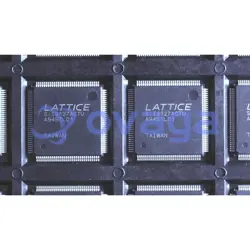
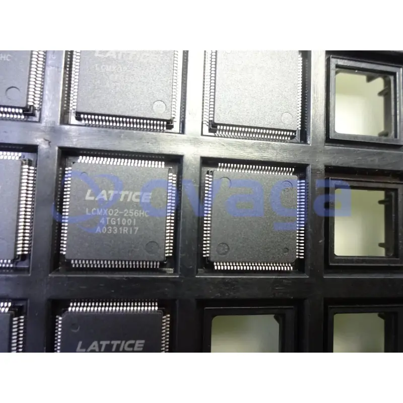
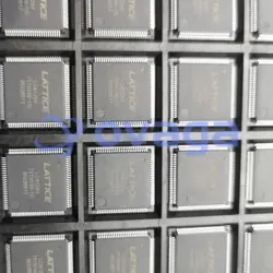
$5000LATTICE LCMXO2-256HC-4TG100I
High component density and flexibility


Marques: Lattice
Pièce Fabricant #: LCMXO2-256HC-4TG100I
Fiche de données: LCMXO2-256HC-4TG100I Fiche de données (PDF)
Colis/Caisse: TQFP-100
type de produit: FPGAs (Field Programmable Gate Array)
Statut RoHS:
État des stocks: 9 458 pièces, nouveau original
Warranty: 1 Year Ovaga Warranty - Find Out More
0
1
LCMXO2-256HC-4TG100I Description générale
The LCMXO2-256HC-4TG100I is a powerful and efficient FPGA designed by Lattice Semiconductor. With its 256 LUTs and 4,000 Logic Cells, this FPGA offers high performance and versatility for a wide range of applications. Its 3.3V single-supply voltage and maximum speed of 311 MHz make it an ideal choice for low-power and high-speed designs. The device also provides various I/O options, including LVCMOS, LVTTL, and LVDS standards, catering to different interface requirements. Housed in a 100-pin TQFP package, the LCMXO2-256HC-4TG100I is compact and suitable for space-constrained designs. Additionally, its RoHS compliance ensures environmental standards are met
Caractéristiques
- Flexible Logic Architecture
- Six devices with 256 to 6864 LUT4s and 19 to 335 I/Os
- Ultra Low Power Devices
- Advanced 65 nm low power process
- As low as 19 µW standby power
- Programmable low swing differential I/Os
- Stand-by mode and other power saving options
- Embedded and Distributed Memory
- Up to 240 Kbits sysMEM™ Embedded Block RAM
- Up to 54 Kbits Distributed RAM
- Dedicated FIFO control logic On-Chip User Flash Memory
- Up to 256 Kbits of User Flash Memory
- 100,000 write cycles
- Accessible through WISHBONE, SPI, I2C and JTAG interfaces
- Can be used as soft processor PROM or as Flash memory
- Pre-Engineered Source Synchronous I/O
- DDR registers in I/O cells
- Dedicated gearing logic
- 7:1 Gearing for Display I/Os
- Generic DDR, DDRX2, DDRX4
- Dedicated DDR/DDR2/LPDDR memory with DQS support
- High Performance, Flexible I/O Buffer
- Programmable sysIO™ buffer supports wide range of interfaces:
- – LVCMOS 3.3/2.5/1.8/1.5/1.2
- – LVTTL
- –PCI
- – LVDS, Bus-LVDS, MLVDS, RSDS, LVPECL
- – SSTL 25/18
- – HSTL 18
- – Schmitt trigger inputs, up to 0.5V hysteresis
- I/Os support hot socketing
- On-chip differential termination
- Programmable pull-up or pull-down mode

Caractéristiques
| Paramètre | Valeur | Paramètre | Valeur |
|---|---|---|---|
| Manufacturer: | Lattice | Product Category: | FPGA - Field Programmable Gate Array |
| RoHS: | Details | Series: | LCMXO2 |
| Number of Logic Elements: | 256 LE | Adaptive Logic Modules - ALMs: | 128 ALM |
| Embedded Memory: | 0 bit | Number of I/Os: | 55 I/O |
| Supply Voltage - Min: | 2.375 V | Supply Voltage - Max: | 3.6 V |
| Minimum Operating Temperature: | - 40 C | Maximum Operating Temperature: | + 100 C |
| Number of Transceivers: | - | Mounting Style: | SMD/SMT |
| Package / Case: | TQFP-100 | Packaging: | Tray |
| Brand: | Lattice | Distributed RAM: | 2 kbit |
| Maximum Operating Frequency: | 269 MHz | Moisture Sensitive: | Yes |
| Number of Logic Array Blocks - LABs: | 32 LAB | Operating Supply Current: | 18 uA |
| Operating Supply Voltage: | 2.5 V/3.3 V | Product Type: | FPGA - Field Programmable Gate Array |
| Factory Pack Quantity: | 90 | Subcategory: | Programmable Logic ICs |
| Total Memory: | 2 kbit | Tradename: | MachXO2 |
| Unit Weight: | 0.023175 oz |
Expédition
| Type d'expédition | Frais d'expédition | Délai de mise en œuvre | |
|---|---|---|---|
 |
DHL | $20.00-$40.00 (0.50 KG) | 2-5 jours |
 |
FedEx | $20.00-$40.00 (0.50 KG) | 2-5 jours |
 |
UPS | $20.00-$40.00 (0.50 KG) | 2-5 jours |
 |
TNT | $20.00-$40.00 (0.50 KG) | 2-5 jours |
 |
EMS | $20.00-$40.00 (0.50 KG) | 2-5 jours |
 |
LA POSTE AÉRIENNE ENREGISTRÉE | $20.00-$40.00 (0.50 KG) | 2-5 jours |
Délai de traitement : les frais d'expédition dépendent des différentes zones et pays.
Paiement
| Modalités de paiement | Frais de main | |
|---|---|---|
 |
Virement bancaire | facturer des frais bancaires de 30,00 $ US. |
 |
Pay Pal | facturer des frais de service de 4,0 %. |
 |
Carte de crédit | facturez des frais de service de 3,5%. |
 |
Western union | charge US.00 banking fee. |
 |
Paiement de Petit Montant | facturer des frais bancaires de 0,00 $ US. |
Garanties
1. Les composants électroniques que vous achetez incluent une garantie de 365 jours, nous garantissons la qualité du produit.
2. Si certains des articles que vous avez reçus ne sont pas de qualité parfaite, nous organiserons de manière responsable votre remboursement ou votre remplacement. Mais les articles doivent rester dans leur état d’origine.
Emballage
-

Étape1 :Produit
-

Étape2 :Emballage sous vide
-

Étape3 :Sac antistatique
-

Étape4 :Emballage individuel
-

Étape5 :Boîtes d'emballage
-

Étape6 :étiquette d'expédition à code-barres


Tous les produits seront emballés dans un sac antistatique. Expédié avec une protection antistatique ESD.
L'étiquette de l'emballage extérieur ESD utilisera les informations de notre société : numéro de pièce, marque et quantité.
Nous inspecterons toutes les marchandises avant expédition, garantirons que tous les produits sont en bon état et que les pièces sont neuves et correspondent à la fiche technique originale.
Une fois que toutes les marchandises sont garanties sans problème après l'emballage, nous les emballerons en toute sécurité et les enverrons par Global Express. Il présente une excellente résistance à la perforation et à la déchirure ainsi qu’une bonne intégrité du joint.


Points de pièce
-
LCMXO2-256HC-4TG100I is a low-cost, low-power Field Programmable Gate Array (FPGA) chip manufactured by Lattice Semiconductor. It offers a range of features, including 256 Look-Up Tables, flexible I/O options, and non-volatile configuration memory. With its compact size and energy-efficient design, this FPGA is suitable for various applications, such as consumer electronics, industrial control systems, and Internet of Things (IoT) devices.
-
Features
LCMXO2-256HC-4TG100I is a low-cost, low-power FPGA from Lattice Semiconductor. It offers 256 LUTs, 2.7Kbits of embedded memory, and 10 I/Os. It operates at a maximum clock frequency of 112 MHz and supports non-volatile flash-based configuration. It is suitable for applications in consumer electronics, industrial control, and automotive sectors. -
Pinout
The LCMXO2-256HC-4TG100I is an FPGA with a pin count of 100 pins. It is a low-cost, low-power device that provides basic programmable functions for various applications, including consumer electronics and wireless communication products. -
Manufacturer
The manufacturer of the LCMXO2-256HC-4TG100I is Lattice Semiconductor Corporation. It is a leading provider of customizable smart connectivity solutions, offering a range of programmable logic devices, software, IP cores, and development kits. Lattice Semiconductor focuses on enabling smarter, more connected applications in various industries, including automotive, consumer electronics, industrial, and communications. -
Application Field
The LCMXO2-256HC-4TG100I is a low-cost, low-power Field-Programmable Gate Array (FPGA) that can be used in various application areas, including consumer electronics, industrial control systems, communications equipment, medical devices, and automotive systems. It offers high performance, flexibility, and low power consumption, making it suitable for a wide range of applications. -
Package
The LCMXO2-256HC-4TG100I chip has a package type of TQFP, a form of Surface Mount, and a size of 10x10mm.


Nous fournissons des produits de haute qualité, un service attentionné et une garantie après-vente
-

Nous avons des produits riches, pouvons répondre à vos différents besoins.
-

La quantité minimum de commande commence à partir de 1 pièce.
-

Les frais d'expédition internationaux les plus bas commencent à partir de 0,00 $
-

Garantie de qualité de 365 jours pour tous les produits