Les images sont à titre de référence uniquement. Voir les spécifications du produit
Commandes de plus de
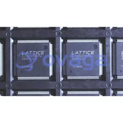
$5000LATTICE LFXP2-17E-5FN484C
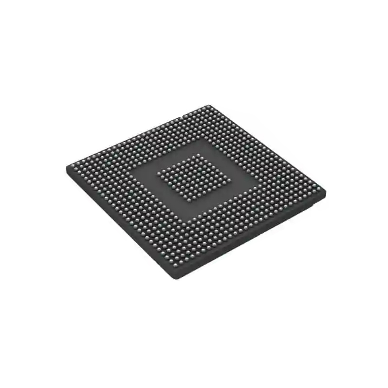
LFXP2-17E-5FN484C is a XP2 Field Programmable Gate Array (FPGA) IC with 358 logic elements and 282624 bits of memory in a 484-BBGA package


Marques: Lattice
Pièce Fabricant #: LFXP2-17E-5FN484C
Fiche de données: LFXP2-17E-5FN484C Fiche de données (PDF)
Colis/Caisse: FPBGA-484
type de produit: FPGAs (Field Programmable Gate Array)
Statut RoHS:
État des stocks: 5 075 pièces, nouveau original
Warranty: 1 Year Ovaga Warranty - Find Out More
0
1
LFXP2-17E-5FN484C Description générale
The LFXP2-17E-5FN484C is a versatile FPGA offering a balance of performance and efficiency. With 17,000 LUTs at its disposal, this FPGA is capable of implementing a wide range of logic functions with ease. Operating at a speedy 352MHz, it ensures smooth and efficient operation for your applications. Its 248 user I/Os provide ample connectivity options for interfacing with external devices, while the 281 embedded block RAMs offer generous storage capacity for your data needs
Caractéristiques
- Fully supports PowerPC™ 60x bus protocol, include PowerPC 603, 604, 740, 750 and 8260.
- Supports up to eight PowerPC bus masters with unlimited slave device support.
- Supports two outstanding bus accesses.
- Supports address only transfer and address bus retry.
- Independent address bus and data bus tenure with separate bus grant and data bus grant.
- Option for fixed priority assignment or rotating priority scheme.
- Designed for ASIC or programmable logic device implementations in various system environments.
- Fully static design with edge triggered flip-flops.
- Optimized for ispXPGA product family.
Caractéristiques
| Paramètre | Valeur | Paramètre | Valeur |
|---|---|---|---|
| Manufacturer | Lattice | Product Category | FPGA - Field Programmable Gate Array |
| RoHS | Details | Series | LFXP2 |
| Number of Logic Elements | 17000 LE | Adaptive Logic Modules - ALMs | 8500 ALM |
| Embedded Memory | 276 kbit | Number of I/Os | 358 I/O |
| Supply Voltage - Min | 1.14 V | Supply Voltage - Max | 1.26 V |
| Minimum Operating Temperature | 0 C | Maximum Operating Temperature | + 85 C |
| Mounting Style | SMD/SMT | Package / Case | FPBGA-484 |
| Brand | Lattice | Distributed RAM | 35 kbit |
| Embedded Block RAM - EBR | 276 kbit | Height | 1.65 mm |
| Length | 23 mm | Maximum Operating Frequency | 311 MHz |
| Moisture Sensitive | Yes | Number of Logic Array Blocks - LABs | 2125 LAB |
| Operating Supply Voltage | 1.2 V | Product Type | FPGA - Field Programmable Gate Array |
| Factory Pack Quantity | 60 | Subcategory | Programmable Logic ICs |
| Total Memory | 311 kbit | Width | 23 mm |
| Unit Weight | 0.077955 oz |
Expédition
| Type d'expédition | Frais d'expédition | Délai de mise en œuvre | |
|---|---|---|---|
 |
DHL | $20.00-$40.00 (0.50 KG) | 2-5 jours |
 |
FedEx | $20.00-$40.00 (0.50 KG) | 2-5 jours |
 |
UPS | $20.00-$40.00 (0.50 KG) | 2-5 jours |
 |
TNT | $20.00-$40.00 (0.50 KG) | 2-5 jours |
 |
EMS | $20.00-$40.00 (0.50 KG) | 2-5 jours |
 |
LA POSTE AÉRIENNE ENREGISTRÉE | $20.00-$40.00 (0.50 KG) | 2-5 jours |
Délai de traitement : les frais d'expédition dépendent des différentes zones et pays.
Paiement
| Modalités de paiement | Frais de main | |
|---|---|---|
 |
Virement bancaire | facturer des frais bancaires de 30,00 $ US. |
 |
Pay Pal | facturer des frais de service de 4,0 %. |
 |
Carte de crédit | facturez des frais de service de 3,5%. |
 |
Western union | charge US.00 banking fee. |
 |
Paiement de Petit Montant | facturer des frais bancaires de 0,00 $ US. |
Garanties
1. Les composants électroniques que vous achetez incluent une garantie de 365 jours, nous garantissons la qualité du produit.
2. Si certains des articles que vous avez reçus ne sont pas de qualité parfaite, nous organiserons de manière responsable votre remboursement ou votre remplacement. Mais les articles doivent rester dans leur état d’origine.
Emballage
-

Étape1 :Produit
-

Étape2 :Emballage sous vide
-

Étape3 :Sac antistatique
-

Étape4 :Emballage individuel
-

Étape5 :Boîtes d'emballage
-

Étape6 :étiquette d'expédition à code-barres


Tous les produits seront emballés dans un sac antistatique. Expédié avec une protection antistatique ESD.
L'étiquette de l'emballage extérieur ESD utilisera les informations de notre société : numéro de pièce, marque et quantité.
Nous inspecterons toutes les marchandises avant expédition, garantirons que tous les produits sont en bon état et que les pièces sont neuves et correspondent à la fiche technique originale.
Une fois que toutes les marchandises sont garanties sans problème après l'emballage, nous les emballerons en toute sécurité et les enverrons par Global Express. Il présente une excellente résistance à la perforation et à la déchirure ainsi qu’une bonne intégrité du joint.


Points de pièce
-
The LFXP2-17E-5FN484C is a high-performance programmable logic device (PLD) produced by Lattice Semiconductor. It features 1684 Look-Up Tables (LUTs), 269 I/Os, and is configured with non-volatile Flash technology. This chip is ideal for a variety of applications in industries such as telecommunications, industrial automation, and automotive.
-
Equivalent
The equivalent products of LFXP2-17E-5FN484C chip are LFXP2-5E-5FTN256C, LFXP2-5E-6TN144C, LFXP2-5E-7FTN144C. -
Features
LFXP2-17E-5FN484C is a low-power, low-cost, and small-size FPGA with 1,700 Look-Up Tables (LUTs) and 64 kbits of embedded SRAM. It features 17 I/Os, 5 V tolerance, and operates at a speed grade of -5, making it suitable for various applications requiring programmable logic solutions. -
Pinout
LFXP2-17E-5FN484C is a 48-pin FPGA (Field-Programmable Gate Array) with 17,056 Look-Up Tables (LUTs), 1.8V core voltage, and 484-ball FineLine BGA package. Its functions include programmable logic, I/O configuration, and user-accessible connection points for designing custom digital circuits. -
Manufacturer
LFXP2-17E-5FN484C is manufactured by Lattice Semiconductor Corporation, which is a multinational company specializing in programmable logic devices, including field-programmable gate arrays (FPGAs) and programmable mixed-signal devices. Lattice Semiconductor provides solutions for a wide range of industries, including automotive, consumer electronics, and industrial applications. -
Application Field
The LFXP2-17E-5FN484C is a low-power, reconfigurable FPGA suitable for applications in industrial automation, IoT devices, sensor networks, and communication systems. It can also be used in consumer electronics, medical devices, and automotive systems where low power consumption and high performance are required. -
Package
The LFXP2-17E-5FN484C chip is a Field Programmable Gate Array (FPGA) in a FineLine BGA package. It has a form factor of 484-pin and a size of 23mm x 23mm.


Nous fournissons des produits de haute qualité, un service attentionné et une garantie après-vente
-

Nous avons des produits riches, pouvons répondre à vos différents besoins.
-

La quantité minimum de commande commence à partir de 1 pièce.
-

Les frais d'expédition internationaux les plus bas commencent à partir de 0,00 $
-

Garantie de qualité de 365 jours pour tous les produits