Les images sont à titre de référence uniquement. Voir les spécifications du produit
Commandes de plus de
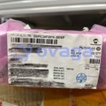
$5000LFXP2-8E-5TN144I
FPGA with 8K LUTs and 100 I/O instances for DSP applications at 1.2V and -5 speed grade


Marques: Lattice
Pièce Fabricant #: LFXP2-8E-5TN144I
Fiche de données: LFXP2-8E-5TN144I Fiche de données (PDF)
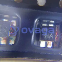
Colis/Caisse: TQFP-144
type de produit: FPGAs (Field Programmable Gate Array)
Statut RoHS:
État des stocks: 9 220 pièces, nouveau original
Warranty: 1 Year Ovaga Warranty - Find Out More
0
1
LFXP2-8E-5TN144I Description générale
Lattice Semiconductor's LFXP2-8E-5TN144I is a standout member of the LatticeXP2 family, offering impressive features in a compact form factor. With its high logic capacity, low-power design, and support for various I/O standards, this FPGA provides a versatile and efficient solution for a wide range of applications. Its high-speed performance and embedded memory blocks make it a compelling choice for projects that require quick data processing and storage
Caractéristiques
- The LFXP2-8E-5TN144I has a unique architecture that supports parallel processing
- This enables high-speed data transfer between different parts of the FPGA
- The device also includes advanced power management features
- This enables efficient use of energy and reduces heat generation
- The LFXP2-8E-5TN144I is suitable for a wide range of applications
Application
- Small but mighty
- Powerful and efficient
- Perfect for IoT
Caractéristiques
| Paramètre | Valeur | Paramètre | Valeur |
|---|---|---|---|
| Product Category | FPGA - Field Programmable Gate Array | RoHS | Details |
| Series | LFXP2 | Number of Logic Elements | 8000 LE |
| Adaptive Logic Modules - ALMs | 4000 ALM | Embedded Memory | 221 kbit |
| Number of I/Os | 100 I/O | Supply Voltage - Min | 1.14 V |
| Supply Voltage - Max | 1.26 V | Minimum Operating Temperature | - 40 C |
| Maximum Operating Temperature | + 100 C | Mounting Style | SMD/SMT |
| Package / Case | TQFP-144 | Brand | Lattice |
| Distributed RAM | 18 kbit | Embedded Block RAM - EBR | 221 kbit |
| Height | 1.4 mm | Length | 20 mm |
| Maximum Operating Frequency | 311 MHz | Moisture Sensitive | Yes |
| Number of Logic Array Blocks - LABs | 1000 LAB | Operating Supply Voltage | 1.2 V |
| Product Type | FPGA - Field Programmable Gate Array | Factory Pack Quantity | 60 |
| Subcategory | Programmable Logic ICs | Total Memory | 239 kbit |
| Width | 20 mm |
Expédition
| Type d'expédition | Frais d'expédition | Délai de mise en œuvre | |
|---|---|---|---|
 |
DHL | $20.00-$40.00 (0.50 KG) | 2-5 jours |
 |
FedEx | $20.00-$40.00 (0.50 KG) | 2-5 jours |
 |
UPS | $20.00-$40.00 (0.50 KG) | 2-5 jours |
 |
TNT | $20.00-$40.00 (0.50 KG) | 2-5 jours |
 |
EMS | $20.00-$40.00 (0.50 KG) | 2-5 jours |
 |
LA POSTE AÉRIENNE ENREGISTRÉE | $20.00-$40.00 (0.50 KG) | 2-5 jours |
Délai de traitement : les frais d'expédition dépendent des différentes zones et pays.
Paiement
| Modalités de paiement | Frais de main | |
|---|---|---|
 |
Virement bancaire | facturer des frais bancaires de 30,00 $ US. |
 |
Pay Pal | facturer des frais de service de 4,0 %. |
 |
Carte de crédit | facturez des frais de service de 3,5%. |
 |
Western union | charge US.00 banking fee. |
 |
Paiement de Petit Montant | facturer des frais bancaires de 0,00 $ US. |
Garanties
1. Les composants électroniques que vous achetez incluent une garantie de 365 jours, nous garantissons la qualité du produit.
2. Si certains des articles que vous avez reçus ne sont pas de qualité parfaite, nous organiserons de manière responsable votre remboursement ou votre remplacement. Mais les articles doivent rester dans leur état d’origine.
Emballage
-

Étape1 :Produit
-

Étape2 :Emballage sous vide
-

Étape3 :Sac antistatique
-

Étape4 :Emballage individuel
-

Étape5 :Boîtes d'emballage
-

Étape6 :étiquette d'expédition à code-barres


Tous les produits seront emballés dans un sac antistatique. Expédié avec une protection antistatique ESD.
L'étiquette de l'emballage extérieur ESD utilisera les informations de notre société : numéro de pièce, marque et quantité.
Nous inspecterons toutes les marchandises avant expédition, garantirons que tous les produits sont en bon état et que les pièces sont neuves et correspondent à la fiche technique originale.
Une fois que toutes les marchandises sont garanties sans problème après l'emballage, nous les emballerons en toute sécurité et les enverrons par Global Express. Il présente une excellente résistance à la perforation et à la déchirure ainsi qu’une bonne intégrité du joint.


Points de pièce
-
The LFXP2-8E-5TN144I chip is a low-cost and low-power FPGA (Field-Programmable Gate Array) from Lattice Semiconductor aimed at applications requiring high-performance and flexibility. With 2,320 LUTs and 10,000 logic elements, this chip offers a versatile platform for implementing various designs and algorithms. Its compact size and low power consumption make it suitable for embedded systems and IoT applications.
-
Equivalent
The equivalent products of LFXP2-8E-5TN144I chip are LFE2-8E-5TN144, LFE2-8E-6TN, and LFE2-8E-7FT256. These chips are from the same Lattice Semiconductor family and have similar features and functionality, making them suitable replacements for the LFXP2-8E-5TN144I chip. -
Features
The LFXP2-8E-5TN144I is a low-power, small-footprint FPGA with 1550 logic elements, 48 Kbits of block RAM, and 37 user I/Os. It features Flash*Freeze technology for ultra-low static power consumption, In-System Programming (ISP) capability, and reconfigurable logic module (RLM) blocks for flexible design implementation. -
Pinout
The LFXP2-8E-5TN144I is a 144-pin FPGA (field-programmable gate array) with 8K LUTs and 108 I/Os. It is used for implementing digital logic circuits and customizing functions. The pin count refers to the number of I/O pins connecting the device to external components for input and output operations. -
Manufacturer
The manufacturer of the LFXP2-8E-5TN144I is Lattice Semiconductor Corporation. It is a technology company that specializes in semiconductor design and manufacturing. Lattice Semiconductor Corporation focuses on developing programmable logic devices, software, and related intellectual property to help customers build innovative products across a wide range of markets. -
Application Field
The LFXP2-8E-5TN144I is suitable for various applications such as industrial automation, medical devices, consumer electronics, communication systems, and automotive electronics. It is an ideal choice for applications that require low power consumption, high performance, and flexibility in a compact form factor. -
Package
The LFXP2-8E-5TN144I chip is in a 144-pin TQFP (Thin Quad Flat Package) form, which measures 14mm x 14mm. The package size is 16mm x 16mm x 1.4mm, and it has 144 pins in a 12x12 grid array.


Nous fournissons des produits de haute qualité, un service attentionné et une garantie après-vente
-

Nous avons des produits riches, pouvons répondre à vos différents besoins.
-

La quantité minimum de commande commence à partir de 1 pièce.
-

Les frais d'expédition internationaux les plus bas commencent à partir de 0,00 $
-

Garantie de qualité de 365 jours pour tous les produits