


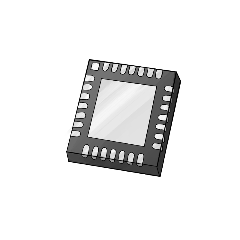
Les images sont à titre de référence uniquement. Voir les spécifications du produit
ON NB4N855SMR4G
Receiver, Driver, Buffer, Translator IC 10-Micro


Marques: ON Semiconductor, LLC
Pièce Fabricant #: NB4N855SMR4G
Fiche de données: NB4N855SMR4G Datasheet (PDF)
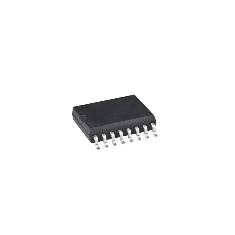
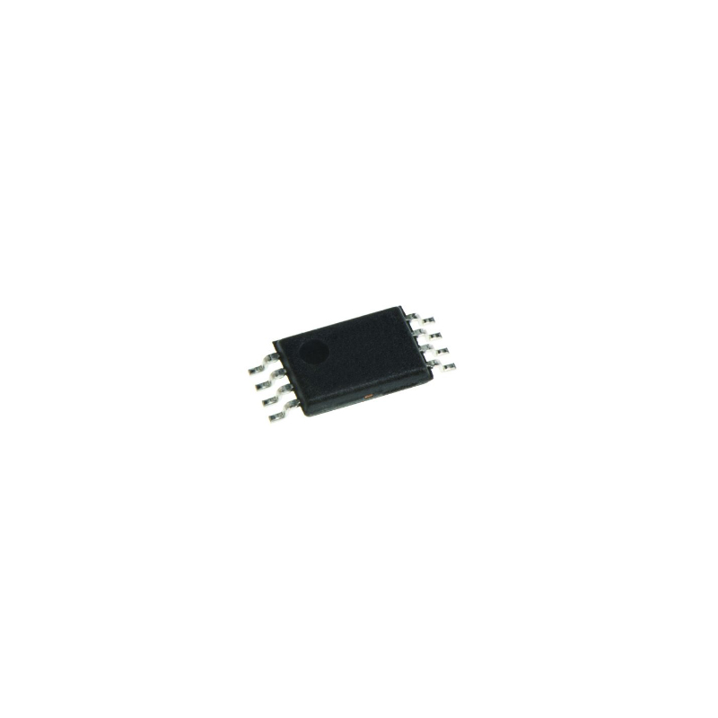
Colis/Caisse: MSOP-10
type de produit: CI logiques
Statut RoHS:
État des stocks: 3031 pièces, nouveau original
Warranty: 1 Year Ovaga Warranty - Find Out More
0
1
Ajouter à la nomenclatureNB4N855SMR4G Description générale
NB4N855S is a clock or data Receiver/Driver/Buffer/Translator capable of translating AnyLevelTM input signal (LVPECL, CML, HSTL, LVDS, or LVTTL/LVCMOS) to LVDS. Depending on the distance, noise immunity of the system design, and transmission line media, this device will receive, drive or translate data or clock signals up to 1.5 Gb/s or 1.0 GHz, respectively. This device is pin-for-pin plug in compatible to the SY55855V in a 3.3 V applications.
The NB4N855S has a wide input common mode range of GND + 50 mV to VCC - 50 mV. This feature is ideal for translating differential or single-ended data or clock signals to 350 mV typical LVDS output levels.
The device is offered in a small 10 lead MSOP package. NB4N855S is targeted for data, wireless and telecom applications as well as high speed logic interface where jitter and package size are main requirements.
Caractéristiques
- Guaranteed Input Clock Frequency up to 1.0 GHz
- Guaranteed Input Data Rate up to 1.5 Gb/s
- 490 ps Maximum Propagation Delay
- 1.0 ps Maximum RMS Jitter
- 180 ps Maximum Rise/Fall Times
- Single Power Supply; VCC = 3.3 V ±10%
- Temperature Compensated TIA/EIA-644 Compliant LVDS Outputs
- GND + 50 mV to VCC - 50 mV VCMR Range
- Pb-Free Packages is Available
Application
- Translation of all major signal types to LVDS in heterogenous systems.
- Signal driving and reception in communications and networking applications.
Caractéristiques
| Paramètre | Valeur | Paramètre | Valeur |
|---|---|---|---|
| Status | Active | CAD Models | |
| Compliance | PbAHP | Package Type | Micro10 |
| Case Outline | 846B | MSL Type | 1 |
| MSL Temp (°C) | 260 | Container Type | REEL |
| Container Qty. | 1000 | ON Target | Y |
| Type | Signal Driver | Channels | 2 |
| Input / Output Ratio | 1:1 | Input Level | TTL |
| Output Level | LVDS | VCC Typ (V) | 3.3 |
| tJitterRMS Typ (ps) | 0.5 | tskew(o-o) Max (ps) | 35 |
| tpd Typ (ns) | 0.41 | tR & tF Max (ps) | 180 |
| fmaxClock Typ (MHz) | 1500 | fmaxData Typ (Mbps) | 2500 |
| Pricing ($/Unit) | Price N/A | feature-logic-family | |
| feature-logic-function | Level Translator | feature-number-of-elements-per-chip | |
| feature-process-technology | feature-maximum-operating-supply-voltage-v | 3.63 | |
| feature-maximum-high-level-output-current-ma | feature-output-type | ||
| feature-maximum-low-level-output-current-ma | feature-packaging | Tape and Reel | |
| feature-minimum-operating-supply-voltage-v | 2.97 | feature-rad-hard | |
| feature-pin-count | 10 | feature-supplier-package | Micro |
| feature-standard-package-name1 | SOP | feature-cecc-qualified | No |
| feature-esd-protection | Yes | feature-military | No |
| feature-aec-qualified | No | feature-aec-qualified-number | |
| feature-auto-motive | No | feature-p-pap | No |
| feature-eccn-code | EAR99 | feature-svhc | No |
| feature-svhc-exceeds-threshold | No |
Expédition
| Type d'expédition | Frais d'expédition | Délai de mise en œuvre | |
|---|---|---|---|
 |
DHL | $20.00-$40.00 (0.50 KG) | 2-5 jours |
 |
FedEx | $20.00-$40.00 (0.50 KG) | 2-5 jours |
 |
UPS | $20.00-$40.00 (0.50 KG) | 2-5 jours |
 |
TNT | $20.00-$40.00 (0.50 KG) | 2-5 jours |
 |
EMS | $20.00-$40.00 (0.50 KG) | 2-5 jours |
 |
LA POSTE AÉRIENNE ENREGISTRÉE | $20.00-$40.00 (0.50 KG) | 2-5 jours |
Délai de traitement : les frais d'expédition dépendent des différentes zones et pays.
Paiement
| Modalités de paiement | Frais de main | |
|---|---|---|
 |
Virement bancaire | facturer des frais bancaires de 30,00 $ US. |
 |
Pay Pal | facturer des frais de service de 4,0 %. |
 |
Carte de crédit | facturez des frais de service de 3,5%. |
 |
Western union | charge US.00 banking fee. |
 |
Paiement de Petit Montant | facturer des frais bancaires de 0,00 $ US. |
Garanties
1. Les composants électroniques que vous achetez incluent une garantie de 365 jours, nous garantissons la qualité du produit.
2. Si certains des articles que vous avez reçus ne sont pas de qualité parfaite, nous organiserons de manière responsable votre remboursement ou votre remplacement. Mais les articles doivent rester dans leur état d’origine.
Emballage
-

Étape1 :Produit
-

Étape2 :Emballage sous vide
-

Étape3 :Sac antistatique
-

Étape4 :Emballage individuel
-

Étape5 :Boîtes d'emballage
-

Étape6 :étiquette d'expédition à code-barres


Tous les produits seront emballés dans un sac antistatique. Expédié avec une protection antistatique ESD.
L'étiquette de l'emballage extérieur ESD utilisera les informations de notre société : numéro de pièce, marque et quantité.
Nous inspecterons toutes les marchandises avant expédition, garantirons que tous les produits sont en bon état et que les pièces sont neuves et correspondent à la fiche technique originale.
Une fois que toutes les marchandises sont garanties sans problème après l'emballage, nous les emballerons en toute sécurité et les enverrons par Global Express. Il présente une excellente résistance à la perforation et à la déchirure ainsi qu’une bonne intégrité du joint.


Points de pièce
-
NB4N855SMR4G is a high-speed, low-power differential receiver chip widely used in applications like fiber optics, data communications, and Clock and Data Recovery systems. It operates at speeds up to 2.7 Gbps and supports a wide input voltage range. With its small size and low power consumption, the chip is an efficient solution for high-speed data transmission in various electronic devices.
-
Equivalent
There are no direct equivalent products to the NB4N855SMR4G chip. However, alternative options for clock and data management include devices like the NB4N527SMR4G and NB4N527SMR4G by ON Semiconductor, and the CDCLVC1104RGZT and CDCLVC1103RGZT by Texas Instruments. -
Features
The NB4N855SMR4G is a clock generator and fanout buffer chip. It offers four universal 1-to-4 fanout buffers with differential input options and dedicated select (SEL) pins for each output bank. The chip operates at a wide range of input frequencies, provides low phase noise and jitter, and has a small package size. -
Pinout
The NB4N855SMR4G is a 16-pin clock and data retiming repeater. It functions as a high-speed differential signal receiver and driver. -
Manufacturer
The manufacturer of the NB4N855SMR4G is ON Semiconductor, an American company specializing in semiconductor manufacturing. -
Application Field
The NB4N855SMR4G is a high-speed differential clock and data fan-out buffer designed for applications requiring high-performance signal distribution with minimal power consumption. It is commonly used in communication systems, networking equipment, data centers, and other applications where reliable clock and data distribution is critical for system operation. -
Package
The NB4N855SMR4G chip comes in a TSSOP-8 package with a form factor of 3.00mm x 4.40mm.
Fiche de données PDF
Nous fournissons des produits de haute qualité, un service attentionné et une garantie après-vente
-

Nous avons des produits riches, pouvons répondre à vos différents besoins.
-

La quantité minimum de commande commence à partir de 1 pièce.
-

Les frais d'expédition internationaux les plus bas commencent à partir de 0,00 $
-

Garantie de qualité de 365 jours pour tous les produits


Top-notch quality components that exceeded my expectations.