

Les images sont à titre de référence uniquement. Voir les spécifications du produit
ON NC7WV07P6X
Buffer, Non-Inverting 2 Element 1 Bit per Element Open Drain Output SC-88 (SC-70-6)


Marques: ON Semiconductor, LLC
Pièce Fabricant #: NC7WV07P6X
Fiche de données: NC7WV07P6X Datasheet (PDF)
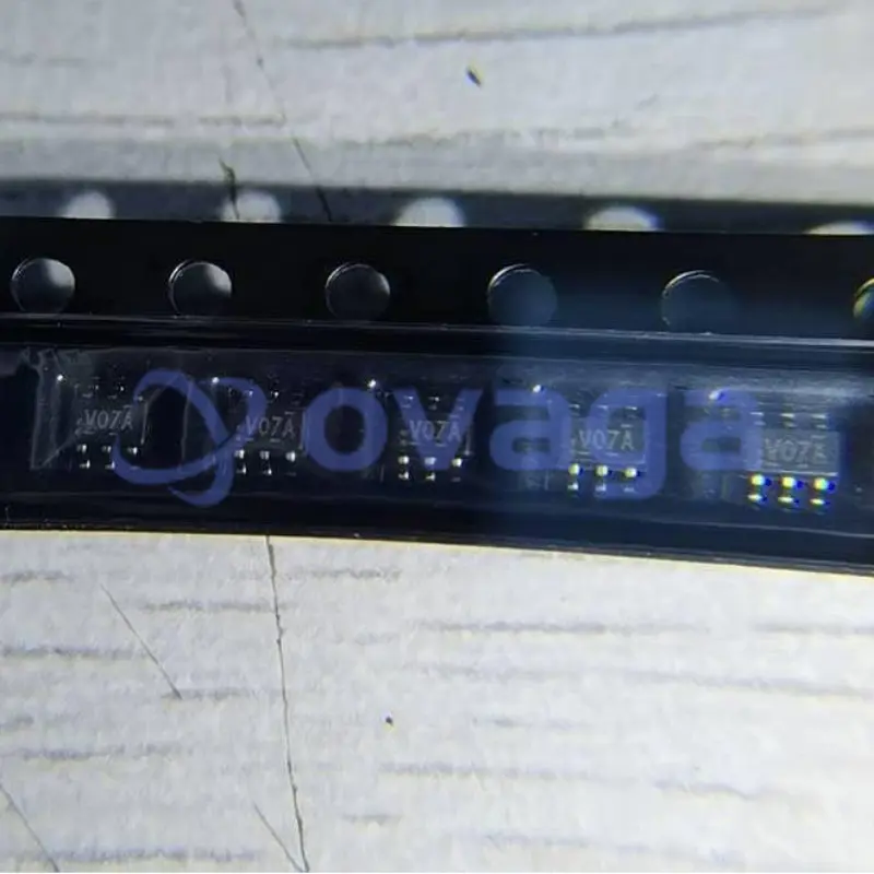
Colis/Caisse: SC-70-6
type de produit: CI logiques
Statut RoHS:
État des stocks: 3547 pièces, nouveau original
Warranty: 1 Year Ovaga Warranty - Find Out More
0
1
Ajouter à la nomenclatureNC7WV07P6X Description générale
The NC7WV07 is a dual buffer with open drain output from ON Semiconductor's Ultra Low Power-A series of TinyLogic®. ULP-A is ideal for applications that require extreme high speed, high drive and low power. This product is designed for a wide low voltage operating range (0.9V to 3.6V VCC) and applications that require more drive and speed than the TinyLogic ULP series, but still offer best in class low power operation.
The NC7WV07 is uniquely designed for optimized power and speed, and is fabricated with an advanced CMOS technology to achieve high-speed operation while maintaining low CMOS power dissipation.
Caractéristiques
- 0.9V to 3.6V VCC supply operation
- 3.6V overvoltage tolerant I/O's at VCC from 0.9V to 3.6V
- Extremely High Speed tPD1.0 ns typ for 2.7V to 3.6V VCC1.2 ns typ for 2.3V to 2.7V VCC2.0 ns typ for 1.65V to 1.95V VCC3.2 ns typ for 1.4V to 1.6V VCC6.0 ns typ for 1.1V to 1.3V VCC13.0 ns typ for 0.9V VCC
- Power-Off high impedance inputs and outputs
- High Static Drive (IOH/IOL)±24 mA @ 3.00V VCC±18 mA @ 2.30V VCC±6 mA @ 1.65V VCC±4 mA @ 1.4V VCC±2 mA @ 1.1V VCC±0.1 mA @ 0.9V VCC
- Uses patented Quiet Series™ noise/EMI reduction circuitry
- Ultra small MicroPak™ leadfree package
- Ultra low dynamic power
Application
- This product is general usage and suitable for many different applications.
Caractéristiques
| Paramètre | Valeur | Paramètre | Valeur |
|---|---|---|---|
| Source Content uid | NC7WV07P6X | Pbfree Code | Yes |
| Part Life Cycle Code | Active | Ihs Manufacturer | ONSEMI |
| Package Description | SC-88, 6 PIN | Manufacturer Package Code | 419AD |
| Reach Compliance Code | compliant | HTS Code | 8542.39.00.01 |
| Factory Lead Time | 75 Weeks, 5 Days | Samacsys Manufacturer | onsemi |
| Family | AUP/ULP/V | JESD-30 Code | R-PDSO-G6 |
| Logic IC Type | BUFFER | Moisture Sensitivity Level | 1 |
| Number of Functions | 2 | Number of Inputs | 1 |
| Number of Terminals | 6 | Output Characteristics | OPEN-DRAIN |
| Package Body Material | PLASTIC/EPOXY | Package Code | TSSOP |
| Package Equivalence Code | TSSOP6,.08 | Package Shape | RECTANGULAR |
| Package Style | SMALL OUTLINE, THIN PROFILE, SHRINK PITCH | Packing Method | TR |
| Peak Reflow Temperature (Cel) | 260 | Schmitt Trigger | NO |
| Surface Mount | YES | Technology | CMOS |
| Terminal Finish | NICKEL PALLADIUM GOLD | Terminal Form | GULL WING |
| Terminal Position | DUAL | Time@Peak Reflow Temperature-Max (s) | 30 |
| feature-logic-family | WV | feature-logic-function | Buffer/Driver |
| feature-number-of-elements-per-chip | 2 | feature-process-technology | CMOS |
| feature-maximum-low-level-output-current-ma | 24 | feature-output-type | Open Drain |
| feature-minimum-operating-supply-voltage-v | 0.9 | feature-maximum-operating-supply-voltage-v | 3.6 |
| feature-maximum-high-level-output-current-ma | -24 | feature-packaging | Tape and Reel |
| feature-rad-hard | feature-pin-count | 6 | |
| feature-supplier-package | SC-70 | feature-standard-package-name1 | SOT |
| feature-cecc-qualified | No | feature-esd-protection | |
| feature-military | No | feature-aec-qualified | No |
| feature-aec-qualified-number | feature-auto-motive | No | |
| feature-p-pap | No | feature-eccn-code | EAR99 |
| feature-svhc | No |
Expédition
| Type d'expédition | Frais d'expédition | Délai de mise en œuvre | |
|---|---|---|---|
 |
DHL | $20.00-$40.00 (0.50 KG) | 2-5 jours |
 |
FedEx | $20.00-$40.00 (0.50 KG) | 2-5 jours |
 |
UPS | $20.00-$40.00 (0.50 KG) | 2-5 jours |
 |
TNT | $20.00-$40.00 (0.50 KG) | 2-5 jours |
 |
EMS | $20.00-$40.00 (0.50 KG) | 2-5 jours |
 |
LA POSTE AÉRIENNE ENREGISTRÉE | $20.00-$40.00 (0.50 KG) | 2-5 jours |
Délai de traitement : les frais d'expédition dépendent des différentes zones et pays.
Paiement
| Modalités de paiement | Frais de main | |
|---|---|---|
 |
Virement bancaire | facturer des frais bancaires de 30,00 $ US. |
 |
Pay Pal | facturer des frais de service de 4,0 %. |
 |
Carte de crédit | facturez des frais de service de 3,5%. |
 |
Western union | charge US.00 banking fee. |
 |
Paiement de Petit Montant | facturer des frais bancaires de 0,00 $ US. |
Garanties
1. Les composants électroniques que vous achetez incluent une garantie de 365 jours, nous garantissons la qualité du produit.
2. Si certains des articles que vous avez reçus ne sont pas de qualité parfaite, nous organiserons de manière responsable votre remboursement ou votre remplacement. Mais les articles doivent rester dans leur état d’origine.
Emballage
-

Étape1 :Produit
-

Étape2 :Emballage sous vide
-

Étape3 :Sac antistatique
-

Étape4 :Emballage individuel
-

Étape5 :Boîtes d'emballage
-

Étape6 :étiquette d'expédition à code-barres


Tous les produits seront emballés dans un sac antistatique. Expédié avec une protection antistatique ESD.
L'étiquette de l'emballage extérieur ESD utilisera les informations de notre société : numéro de pièce, marque et quantité.
Nous inspecterons toutes les marchandises avant expédition, garantirons que tous les produits sont en bon état et que les pièces sont neuves et correspondent à la fiche technique originale.
Une fois que toutes les marchandises sont garanties sans problème après l'emballage, nous les emballerons en toute sécurité et les enverrons par Global Express. Il présente une excellente résistance à la perforation et à la déchirure ainsi qu’une bonne intégrité du joint.


Points de pièce
-
The NC7WV07P6X chip is a triple buffer gate that can be used for level shifting signals in various electronic circuits. It has three inputs and three outputs and operates at a supply voltage of 1.65V to 5.5V. The chip is designed to provide high-speed signal buffering while consuming very low power, making it suitable for applications in portable devices and battery-powered systems.
-
Equivalent
There aren't any exact equivalent products to the NC7WV07P6X chip. However, some similar alternatives you may consider are the SN74LV07A, TC7WG07FK, and HCT07 chips, as they have similar functionalities and specifications. -
Features
The NC7WV07P6X is a dual buffer/line driver that operates from rail-to-rail voltage signals with a wide operating voltage range. It offers low power consumption, high-speed operation, and is designed with Schmitt-trigger inputs to provide noise immunity. It also has balanced input and output characteristics and supports overvoltage-tolerant input levels, making it suitable for various applications. -
Pinout
The NC7WV07P6X is a single logic gate with an open-drain output. It has a pin count of 6, which includes one input pin, one output pin, and four power supply/GND pins. The open-drain output allows for bi-directional signal transmission and is commonly used for level shifting applications. -
Manufacturer
The manufacturer of the NC7WV07P6X is ON Semiconductor. ON Semiconductor is a multinational company specializing in the design and production of semiconductors and integrated circuits for various industries, including automotive, communications, computing, and consumer electronics. -
Application Field
The NC7WV07P6X is a voltage-level translator used for translating voltage levels between different logic families. It can be applied in various applications such as battery-powered portable devices, mobile phones, digital cameras, and other electronics requiring voltage translation between different logic levels. -
Package
The NC7WV07P6X chip has a package type of SC-70, a form of SMD (Surface Mount Device), and a size of 2.00mm x 2.10mm x 1.20mm.


Fiche de données PDF
Nous fournissons des produits de haute qualité, un service attentionné et une garantie après-vente
-

Nous avons des produits riches, pouvons répondre à vos différents besoins.
-

La quantité minimum de commande commence à partir de 1 pièce.
-

Les frais d'expédition internationaux les plus bas commencent à partir de 0,00 $
-

Garantie de qualité de 365 jours pour tous les produits


We will definitely be purchasing from Ovaga in the future.