


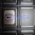
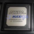
Les images sont à titre de référence uniquement. Voir les spécifications du produit
Commandes de plus de
$5000Altera EP1K50FI256-2
PLD device with fast 0.4ns load time


Marques: Intel
Pièce Fabricant #: EP1K50FI256-2
Fiche de données: EP1K50FI256-2 Datasheet (PDF)
Colis/Caisse: FBGA-256
type de produit: FPGAs (Field Programmable Gate Array)
Statut RoHS:
État des stocks: 2 723 pièces, nouveau original
Warranty: 1 Year Ovaga Warranty - Find Out More
0
1
EP1K50FI256-2 Description générale
The EP1K50FI256-2 from Altera Cyclone is a versatile FPGA featuring 1,500 logic elements and 2,500 gates, making it suitable for a wide range of digital design applications. Its 2.5V core voltage and 256 Kb of embedded memory make it a powerful and efficient choice for telecommunications, industrial automation, and consumer electronics. With support for up to 101 user I/O pins and dedicated hardware multipliers for DSP applications, this FPGA offers flexibility and performance. Its FineLine BGA package provides a compact form factor for easy integration into various systems, while its programmable architecture allows for customizable designs tailored to specific needs. Whether it's for implementing complex algorithms or processing data in real-time, the EP1K50FI256-2 offers the agility and power needed for demanding tasks. Its support for various configuration methods, such as serial configuration devices or configuration via the JTAG interface, ensures seamless integration and easy setup
Caractéristiques
- 50,000 logic elements
- 1,008 kilobits of embedded memory
- 266 user I/O pins
- 333 MHz maximum operating frequency
- 2.5V core voltage
Application
- Digital signal processing (DSP)
- Image and video processing
- Industrial control systems
- Networking and telecommunications
- Test and measurement equipment

Caractéristiques
| Paramètre | Valeur | Paramètre | Valeur |
|---|---|---|---|
| feature-family-name | ACEX 1K | feature-process-technology | 0.22um |
| feature-maximum-number-of-user-i-os | 186 | feature-number-of-registers | |
| feature-device-logic-cells | 2880 | feature-device-system-gates | 199000 |
| feature-number-of-multipliers | feature-program-memory-type | SRAM | |
| feature-ram-bits-kbit | 40 | feature-total-number-of-block-ram | 10 |
| feature-ethernet-macs | feature-supported-ip-core | ||
| feature-supported-ip-core-manufacture | feature-maximum-number-of-serdes-channels | ||
| feature-device-logic-units | 2880 | feature-device-number-of-dlls-plls | 1 |
| feature-transceiver-blocks | feature-transceiver-speed-gbps | ||
| feature-dedicated-dsp | feature-pci-blocks | ||
| feature-programmability | No | feature-maximum-internal-frequency-mhz | 200 |
| feature-speed-grade | 2 | feature-giga-multiply-accumulates-per-second | |
| feature-differential-i-o-standards-supported | feature-single-ended-i-o-standards-supported | LVTTL|LVCMOS | |
| feature-external-memory-interface | feature-minimum-operating-supply-voltage-v | 2.375 | |
| feature-maximum-operating-supply-voltage-v | 2.625 | feature-packaging | |
| feature-rohs | feature-rad-hard | ||
| feature-pin-count | 256 | feature-supplier-package | FBGA |
| feature-standard-package-name1 | BGA | feature-cecc-qualified | No |
| feature-esd-protection | feature-escc-qualified | ||
| feature-military | No | feature-aec-qualified | No |
| feature-aec-qualified-number | feature-auto-motive | No | |
| feature-p-pap | No | feature-eccn-code | 3A991 |
| feature-svhc | Yes |
Expédition
| Type d'expédition | Frais d'expédition | Délai de mise en œuvre | |
|---|---|---|---|
 |
DHL | $20.00-$40.00 (0.50 KG) | 2-5 jours |
 |
FedEx | $20.00-$40.00 (0.50 KG) | 2-5 jours |
 |
UPS | $20.00-$40.00 (0.50 KG) | 2-5 jours |
 |
TNT | $20.00-$40.00 (0.50 KG) | 2-5 jours |
 |
EMS | $20.00-$40.00 (0.50 KG) | 2-5 jours |
 |
LA POSTE AÉRIENNE ENREGISTRÉE | $20.00-$40.00 (0.50 KG) | 2-5 jours |
Délai de traitement : les frais d'expédition dépendent des différentes zones et pays.
Paiement
| Modalités de paiement | Frais de main | |
|---|---|---|
 |
Virement bancaire | facturer des frais bancaires de 30,00 $ US. |
 |
Pay Pal | facturer des frais de service de 4,0 %. |
 |
Carte de crédit | facturez des frais de service de 3,5%. |
 |
Western union | charge US.00 banking fee. |
 |
Paiement de Petit Montant | facturer des frais bancaires de 0,00 $ US. |
Garanties
1. Les composants électroniques que vous achetez incluent une garantie de 365 jours, nous garantissons la qualité du produit.
2. Si certains des articles que vous avez reçus ne sont pas de qualité parfaite, nous organiserons de manière responsable votre remboursement ou votre remplacement. Mais les articles doivent rester dans leur état d’origine.
Emballage
-

Étape1 :Produit
-

Étape2 :Emballage sous vide
-

Étape3 :Sac antistatique
-

Étape4 :Emballage individuel
-

Étape5 :Boîtes d'emballage
-

Étape6 :étiquette d'expédition à code-barres


Tous les produits seront emballés dans un sac antistatique. Expédié avec une protection antistatique ESD.
L'étiquette de l'emballage extérieur ESD utilisera les informations de notre société : numéro de pièce, marque et quantité.
Nous inspecterons toutes les marchandises avant expédition, garantirons que tous les produits sont en bon état et que les pièces sont neuves et correspondent à la fiche technique originale.
Une fois que toutes les marchandises sont garanties sans problème après l'emballage, nous les emballerons en toute sécurité et les enverrons par Global Express. Il présente une excellente résistance à la perforation et à la déchirure ainsi qu’une bonne intégrité du joint.


Points de pièce
-
The EP1K50FI256-2 chip is an FPGA (Field-Programmable Gate Array) manufactured by Altera. It is designed for embedded applications and offers 50,000 logic elements and 1,620 kilobits of embedded memory. It features a high-speed interface and low power consumption, providing flexibility and efficiency in system development.
-
Equivalent
Comparable products of the EP1K50FI256-2 chip include EP1K50QC208-2, EP1K50FC256-2, and EP1K50FC256-1 chips. -
Features
EP1K50FI256-2 is an Altera EP1K FPGA device with 50,000 logic elements, 2,048 Kbits of memory, 268 I/O pins, and operates at a speed grade of -2, supporting a maximum of 200 MHz performance. Additionally, it has built-in PLLs, arithmetic and multiplier blocks, and supports legacy configuration modes. -
Pinout
The EP1K50FI256-2 is an Altera EP1K series field-programmable gate array (FPGA) with a pin count of 256. It has a variety of functions, including digital signal processing (DSP), embedded processing, and general-purpose logic applications. -
Manufacturer
The manufacturer of the EP1K50FI256-2 is Altera Corporation. Altera is a semiconductor company that specializes in the design and manufacturing of programmable logic devices, including field-programmable gate arrays (FPGAs). They provide solutions for various markets such as automotive, communications, industrial, and consumer electronics. -
Application Field
The EP1K50FI256-2 is a field-programmable gate array (FPGA) designed by Altera. It is typically used in applications that require high-speed signal processing, such as telecommunications, network routing, and digital signal processing. Its versatile architecture and programmability make it suitable for a wide range of applications. -
Package
The EP1K50FI256-2 chip is packaged in plastic. Its form is a Ball Grid Array (BGA) with a ceramic substrate. It has 256 pins and measures 27mm x 27mm in size.


Fiche de données PDF
Nous fournissons des produits de haute qualité, un service attentionné et une garantie après-vente
-

Nous avons des produits riches, pouvons répondre à vos différents besoins.
-

La quantité minimum de commande commence à partir de 1 pièce.
-

Les frais d'expédition internationaux les plus bas commencent à partir de 0,00 $
-

Garantie de qualité de 365 jours pour tous les produits


