Les images sont à titre de référence uniquement. Voir les spécifications du produit
Commandes de plus de
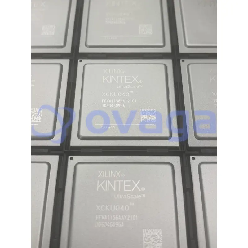
$5000Xilinx XCKU040-2FFVA1156E
Next-generation reconfigurable processor for optimized system architecture


Marques: Xilinx
Pièce Fabricant #: XCKU040-2FFVA1156E
Fiche de données: XCKU040-2FFVA1156E Datasheet (PDF)
Colis/Caisse: FCBGA-1156
type de produit: FPGAs (Field Programmable Gate Array)
Statut RoHS:
État des stocks: 2 454 pièces, nouveau original
Warranty: 1 Year Ovaga Warranty - Find Out More
0
1
XCKU040-2FFVA1156E Description générale
The advanced features of the XCKU040-2FFVA1156E FPGA make it a powerful tool for engineers seeking to push the boundaries of digital design. With its robust logic resources, high-speed interfaces, and efficient use of resources, this FPGA enables the development of innovative solutions that can meet the demands of modern technology
Caractéristiques
- Series: Kintex UltraScale+
- Logic Cells: 363,000
- DSP Slices: 29,400
- Transceivers: 32.5 Gbps
- Device Code: XCKU040-2FFVA11-56E
Application
- Cloud computing
- Audio processing
- Robotics industry

Caractéristiques
| Paramètre | Valeur | Paramètre | Valeur |
|---|---|---|---|
| Product Category | FPGA - Field Programmable Gate Array | RoHS | Details |
| Series | XCKU040 | Number of Logic Elements | 530250 LE |
| Adaptive Logic Modules - ALMs | 30300 ALM | Embedded Memory | 21.1 Mbit |
| Number of I/Os | 520 I/O | Supply Voltage - Min | 922 mV |
| Supply Voltage - Max | 979 mV | Minimum Operating Temperature | 0 C |
| Maximum Operating Temperature | + 100 C | Data Rate | 12.5 Gb/s |
| Number of Transceivers | 20 Transceiver | Mounting Style | SMD/SMT |
| Package / Case | FCBGA-1156 | Brand | Xilinx |
| Distributed RAM | 7 Mbit | Embedded Block RAM - EBR | 21.1 Mbit |
| Moisture Sensitive | Yes | Number of Logic Array Blocks - LABs | 30300 LAB |
| Operating Supply Voltage | 850 mV | Product Type | FPGA - Field Programmable Gate Array |
| Factory Pack Quantity | 1 | Subcategory | Programmable Logic ICs |
| Tradename | Kintex UltraScale |
Expédition
| Type d'expédition | Frais d'expédition | Délai de mise en œuvre | |
|---|---|---|---|
 |
DHL | $20.00-$40.00 (0.50 KG) | 2-5 jours |
 |
FedEx | $20.00-$40.00 (0.50 KG) | 2-5 jours |
 |
UPS | $20.00-$40.00 (0.50 KG) | 2-5 jours |
 |
TNT | $20.00-$40.00 (0.50 KG) | 2-5 jours |
 |
EMS | $20.00-$40.00 (0.50 KG) | 2-5 jours |
 |
LA POSTE AÉRIENNE ENREGISTRÉE | $20.00-$40.00 (0.50 KG) | 2-5 jours |
Délai de traitement : les frais d'expédition dépendent des différentes zones et pays.
Paiement
| Modalités de paiement | Frais de main | |
|---|---|---|
 |
Virement bancaire | facturer des frais bancaires de 30,00 $ US. |
 |
Pay Pal | facturer des frais de service de 4,0 %. |
 |
Carte de crédit | facturez des frais de service de 3,5%. |
 |
Western union | charge US.00 banking fee. |
 |
Paiement de Petit Montant | facturer des frais bancaires de 0,00 $ US. |
Garanties
1. Les composants électroniques que vous achetez incluent une garantie de 365 jours, nous garantissons la qualité du produit.
2. Si certains des articles que vous avez reçus ne sont pas de qualité parfaite, nous organiserons de manière responsable votre remboursement ou votre remplacement. Mais les articles doivent rester dans leur état d’origine.
Emballage
-

Étape1 :Produit
-

Étape2 :Emballage sous vide
-

Étape3 :Sac antistatique
-

Étape4 :Emballage individuel
-

Étape5 :Boîtes d'emballage
-

Étape6 :étiquette d'expédition à code-barres


Tous les produits seront emballés dans un sac antistatique. Expédié avec une protection antistatique ESD.
L'étiquette de l'emballage extérieur ESD utilisera les informations de notre société : numéro de pièce, marque et quantité.
Nous inspecterons toutes les marchandises avant expédition, garantirons que tous les produits sont en bon état et que les pièces sont neuves et correspondent à la fiche technique originale.
Une fois que toutes les marchandises sont garanties sans problème après l'emballage, nous les emballerons en toute sécurité et les enverrons par Global Express. Il présente une excellente résistance à la perforation et à la déchirure ainsi qu’une bonne intégrité du joint.


Pièces équivalentes
Pour le XCKU040-2FFVA1156E composant, vous pouvez envisager ces pièces de rechange et alternatives:
Numéro d'article
Marques
Emballer
Description
Numéro d'article : XCKU040-2FFVA1156E
Marques :
Emballer : 1156-BBGA, FCBGA
Description : There are no direct equivalent parts numbers for the XCKU040-2FFVA1156E as it is a unique FPGA from Xilinx. However, other FPGAs from Xilinx and other manufacturers may offer similar capabilities and can provide alternative options for specific applications.
Points de pièce
-
The XCKU040-2FFVA1156E chip is a versatile field-programmable gate array (FPGA) that belongs to the Xilinx Kintex UltraScale family. It offers a high-performance and low-power solution for various applications, including data center, networking, and aerospace systems. With its advanced features like high-speed transceivers, configurable logic blocks, and embedded memory, the XCKU040-2FFVA1156E chip provides flexibility and scalability in hardware development.
-
Equivalent
There are no direct equivalent products to the XCKU040-2FFVA1156E chip. However, the Xilinx Virtex UltraScale+ family offers similar FPGA chips with varying features and specifications that may be suitable depending on the specific requirements of the application. -
Features
The features of XCKU040-2FFVA1156E include a Xilinx UltraScale+ FPGA, 965,000 logic cells, 5,520 DSP slices, 16.3 Mb of distributed RAM, 40 Mb of block RAM, 96 gigabit transceivers, and 65,520 CLB flip-flops. It also offers 640 digital I/O pins, PCIe Gen3 support, and up to 4.096 Mbits of integrated synchronous RAM. -
Pinout
The XCKU040-2FFVA1156E is a Field Programmable Gate Array (FPGA) with a pin count of 1156. The function of the FPGA can be customized according to user requirements, as it is programmable and can implement various digital logic functions. -
Manufacturer
The XCKU040-2FFVA1156E is manufactured by Xilinx Inc., a semiconductor company that specializes in the development and production of programmable logic devices and related software tools. -
Application Field
The XCKU040-2FFVA1156E is a Field Programmable Gate Array (FPGA) that can be used in various applications such as data center acceleration, wired communication, wireless infrastructure, industrial automation, and aerospace and defense. It offers high-performance computing, low-power capabilities, and advanced features for these application areas. -
Package
The XCKU040-2FFVA1156E chip is available in a Flip Chip Ball Grid Array (FCBGA) package type. It has a form factor of 1156 pins and a size of 35 mm x 35 mm.


Fiche de données PDF
Nous fournissons des produits de haute qualité, un service attentionné et une garantie après-vente
-

Nous avons des produits riches, pouvons répondre à vos différents besoins.
-

La quantité minimum de commande commence à partir de 1 pièce.
-

Les frais d'expédition internationaux les plus bas commencent à partir de 0,00 $
-

Garantie de qualité de 365 jours pour tous les produits