Les images sont à titre de référence uniquement. Voir les spécifications du produit
Commandes de plus de
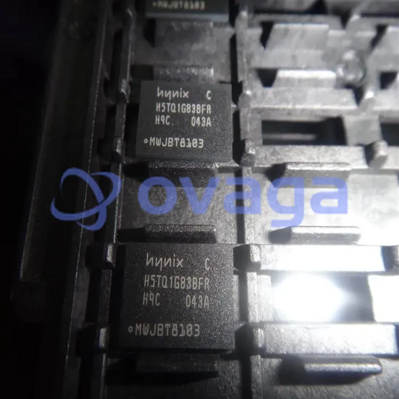
$5000H5TQ1G83BFR-H9C
Enables faster execution of memory-intensive tasks, ensuring smoother performance in various mobile-related operation


Marques: SK HYNIX INC
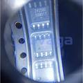
Pièce Fabricant #: H5TQ1G83BFR-H9C
Fiche de données: H5TQ1G83BFR-H9C Fiche de données (PDF)
Colis/Caisse: FBGA-78
type de produit: DRAMs
Statut RoHS:
État des stocks: 6 554 pièces, nouveau original
Warranty: 1 Year Ovaga Warranty - Find Out More
0
1
Caractéristiques
- VDD=VDDQ=1.5V +/- 0.075V
- Fully differential clock inputs (CK, CK) operation
- Differential Data Strobe (DQS, DQS)
- On chip DLL align DQ, DQS and DQS transition with CK
- transition
- DM masks write data-in at the both rising and falling
- edges of the data strobe
- All addresses and control inputs except data,
- data strobes and data masks latched on the
- rising edges of the clock
- Programmable CAS latency 5, 6, 7, 8, 9, 10, 11, 12, 13
- and 14 supported
- Programmable additive latency 0, CL-1, and CL-2
- supported
- Programmable CAS Write latency (CWL) = 5, 6, 7, 8, 9, 10
- Programmable burst length 4/8 with both nibble
- sequential and interleave mode
- BL switch on the fly
- 8banks
- Average Refresh Cycle (Tcase of0 oC~ 95oC)
- - 7.8 µs at 0oC ~ 85 oC
- - 3.9 µs at 85oC ~ 95 oC
- JEDEC standard 78ball FBGA(x4/x8)
- Driver strength selected by EMRS
- Dynamic On Die Termination supported
- Asynchronous RESET pin supported
- ZQ calibration supported
- TDQS (Termination Data Strobe) supported (x8 only)
- Write Levelization supported
- 8 bit pre-fetch
- This product in compliance with the RoHS directive.
Caractéristiques
| Paramètre | Valeur | Paramètre | Valeur |
|---|---|---|---|
| Rohs Code | Yes | Part Life Cycle Code | Obsolete |
| Ihs Manufacturer | SK HYNIX INC | Part Package Code | BGA |
| Package Description | TFBGA, BGA78,9X13,32 | Pin Count | 78 |
| Reach Compliance Code | ECCN Code | EAR99 | |
| HTS Code | 8542.32.00.36 | Access Mode | MULTI BANK PAGE BURST |
| Access Time-Max | 20 ns | Additional Feature | AUTO/SELF REFRESH |
| Clock Frequency-Max (fCLK) | 667 MHz | I/O Type | COMMON |
| Interleaved Burst Length | 4,8 | JESD-30 Code | R-PBGA-B78 |
| JESD-609 Code | e1 | Length | 11 mm |
| Memory Density | 2415919104 bit | Memory IC Type | DDR3 DRAM |
| Memory Width | 18 | Number of Functions | 1 |
| Number of Ports | 1 | Number of Terminals | 78 |
| Number of Words | 134217728 words | Number of Words Code | 128000000 |
| Operating Mode | SYNCHRONOUS | Operating Temperature-Max | 85 °C |
| Operating Temperature-Min | Organization | 128MX18 | |
| Output Characteristics | 3-STATE | Package Body Material | PLASTIC/EPOXY |
| Package Code | TFBGA | Package Equivalence Code | BGA78,9X13,32 |
| Package Shape | RECTANGULAR | Package Style | GRID ARRAY, THIN PROFILE, FINE PITCH |
| Peak Reflow Temperature (Cel) | 260 | Qualification Status | Not Qualified |
| Refresh Cycles | 8192 | Seated Height-Max | 1.2 mm |
| Self Refresh | YES | Sequential Burst Length | 4,8 |
| Supply Current-Max | 0.2 mA | Supply Voltage-Max (Vsup) | 1.575 V |
| Supply Voltage-Min (Vsup) | 1.425 V | Supply Voltage-Nom (Vsup) | 1.5 V |
| Surface Mount | YES | Technology | CMOS |
| Temperature Grade | OTHER | Terminal Finish | Tin/Silver/Copper (Sn96.5Ag3.0Cu0.5) |
| Terminal Form | BALL | Terminal Pitch | 0.8 mm |
| Terminal Position | BOTTOM | Time@Peak Reflow Temperature-Max (s) | 20 |
| Width | 7.5 mm |
Expédition
| Type d'expédition | Frais d'expédition | Délai de mise en œuvre | |
|---|---|---|---|
 |
DHL | $20.00-$40.00 (0.50 KG) | 2-5 jours |
 |
FedEx | $20.00-$40.00 (0.50 KG) | 2-5 jours |
 |
UPS | $20.00-$40.00 (0.50 KG) | 2-5 jours |
 |
TNT | $20.00-$40.00 (0.50 KG) | 2-5 jours |
 |
EMS | $20.00-$40.00 (0.50 KG) | 2-5 jours |
 |
LA POSTE AÉRIENNE ENREGISTRÉE | $20.00-$40.00 (0.50 KG) | 2-5 jours |
Délai de traitement : les frais d'expédition dépendent des différentes zones et pays.
Paiement
| Modalités de paiement | Frais de main | |
|---|---|---|
 |
Virement bancaire | facturer des frais bancaires de 30,00 $ US. |
 |
Pay Pal | facturer des frais de service de 4,0 %. |
 |
Carte de crédit | facturez des frais de service de 3,5%. |
 |
Western union | charge US.00 banking fee. |
 |
Paiement de Petit Montant | facturer des frais bancaires de 0,00 $ US. |
Garanties
1. Les composants électroniques que vous achetez incluent une garantie de 365 jours, nous garantissons la qualité du produit.
2. Si certains des articles que vous avez reçus ne sont pas de qualité parfaite, nous organiserons de manière responsable votre remboursement ou votre remplacement. Mais les articles doivent rester dans leur état d’origine.
Emballage
-

Étape1 :Produit
-

Étape2 :Emballage sous vide
-

Étape3 :Sac antistatique
-

Étape4 :Emballage individuel
-

Étape5 :Boîtes d'emballage
-

Étape6 :étiquette d'expédition à code-barres


Tous les produits seront emballés dans un sac antistatique. Expédié avec une protection antistatique ESD.
L'étiquette de l'emballage extérieur ESD utilisera les informations de notre société : numéro de pièce, marque et quantité.
Nous inspecterons toutes les marchandises avant expédition, garantirons que tous les produits sont en bon état et que les pièces sont neuves et correspondent à la fiche technique originale.
Une fois que toutes les marchandises sont garanties sans problème après l'emballage, nous les emballerons en toute sécurité et les enverrons par Global Express. Il présente une excellente résistance à la perforation et à la déchirure ainsi qu’une bonne intégrité du joint.


Points de pièce
-
The H5TQ1G83BFR-H9C is a chip commonly used in smartphones and other electronic devices. It is a high-performance, low-power DDR3L SDRAM chip manufactured by SK Hynix. With a capacity of 1 gigabit and a frequency of 933 MHz, it provides fast and efficient memory access for improved device performance.
-
Features
H5TQ1G83BFR-H9C is a DDR4 SDRAM chip manufactured by SK Hynix. It has a capacity of 1 gigabit, operates at a speed of 2400 MHz, and is designed to be used in high-performance computing systems. It features low power consumption and high data transfer rates, making it suitable for various applications. -
Pinout
The H5TQ1G83BFR-H9C is a DDR3 SDRAM chip with a pin count of 60. Its main function is to provide storage capacity and fast data transfer rates for computing devices, such as smartphones, tablets, and other electronic devices. -
Manufacturer
H5TQ1G83BFR-H9C is manufactured by SK Hynix, a South Korean semiconductor company. It is one of the world's largest manufacturers of memory chips, including DRAM and NAND flash, and a leading provider of various semiconductor solutions for mobile devices, computers, servers, and more. -
Application Field
The H5TQ1G83BFR-H9C is a high-performance DDR2 SDRAM memory component. It can be used in various electronic devices such as smartphones, tablets, portable gaming consoles, and networking equipment to enhance their memory and processing capabilities. -
Package
The H5TQ1G83BFR-H9C chip has a package type of BGA (Ball Grid Array), a form factor of FBGA (Fine Ball Grid Array), and a size of 11.5mm x 13mm.


Nous fournissons des produits de haute qualité, un service attentionné et une garantie après-vente
-

Nous avons des produits riches, pouvons répondre à vos différents besoins.
-

La quantité minimum de commande commence à partir de 1 pièce.
-

Les frais d'expédition internationaux les plus bas commencent à partir de 0,00 $
-

Garantie de qualité de 365 jours pour tous les produits