

Les images sont à titre de référence uniquement. Voir les spécifications du produit
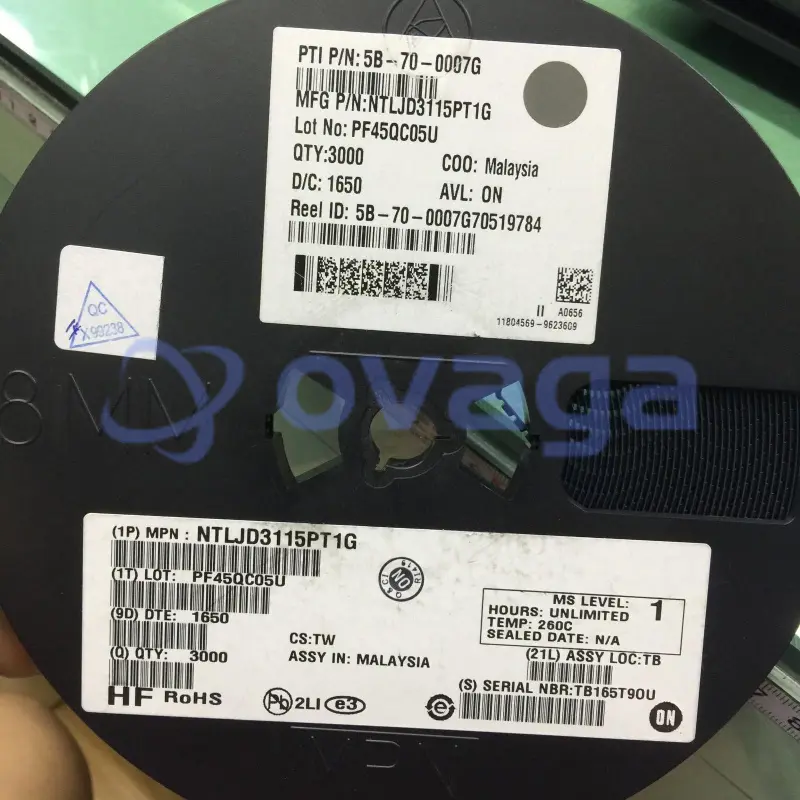
ON NTLJD3115PT1G
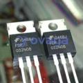
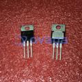
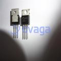
Mosfet Array 20V 2.3A 710mW Surface Mount 6-WDFN (2x2)


Marques: ON Semiconductor, LLC
Pièce Fabricant #: NTLJD3115PT1G
Fiche de données: NTLJD3115PT1G Datasheet (PDF)
Colis/Caisse: WDFN EP
type de produit: Transistors
Statut RoHS:
État des stocks: 3602 pièces, nouveau original
Warranty: 1 Year Ovaga Warranty - Find Out More
0
1
Ajouter à la nomenclatureNTLJD3115PT1G Description générale
Mosfet Array 20V 2.3A 710mW Surface Mount 6-WDFN (2x2)
Caractéristiques
- WDFN Package Provides Exposed Drain Pad for Excellent Thermal Conduction
- 2x2 mm Footprint Same as SC-88
- Lowest RDS(on) Solution in 2x2 mm Package
- 1.8 V RDS(on) Rating for Operation at Low Voltage Gate Drive Logic Level
- Low Profile (< 0.8 mm) for Easy Fit in Thin Environments
- Bidirectional Current Flow with Common Source Configuration
Application
- Optimized for Battery and Load Management Applications in Portable Equipment
- Li-Ion Battery Charging and Protection Circuits
- High Side Load Switch
Caractéristiques
| Paramètre | Valeur | Paramètre | Valeur |
|---|---|---|---|
| Source Content uid | NTLJD3115PT1G | Pbfree Code | Yes |
| Part Life Cycle Code | Active | Ihs Manufacturer | ONSEMI |
| Part Package Code | WDFN6 2x2, 0.65P | Package Description | WDFN-6 |
| Pin Count | 6 | Manufacturer Package Code | 506AN |
| Reach Compliance Code | compliant | ECCN Code | EAR99 |
| Factory Lead Time | 22 Weeks | Samacsys Manufacturer | onsemi |
| Additional Feature | LOGIC LEVEL COMPATIBLE | Case Connection | DRAIN |
| Configuration | SEPARATE, 2 ELEMENTS WITH BUILT-IN DIODE | DS Breakdown Voltage-Min | 20 V |
| Drain Current-Max (ID) | 2.3 A | Drain-source On Resistance-Max | 0.135 Ω |
| FET Technology | METAL-OXIDE SEMICONDUCTOR | JESD-30 Code | S-PDSO-N6 |
| JESD-609 Code | e3 | Moisture Sensitivity Level | 1 |
| Number of Elements | 1 | Number of Terminals | 6 |
| Operating Mode | ENHANCEMENT MODE | Operating Temperature-Max | 150 °C |
| Operating Temperature-Min | -55 °C | Package Body Material | PLASTIC/EPOXY |
| Package Shape | RECTANGULAR | Package Style | SMALL OUTLINE |
| Peak Reflow Temperature (Cel) | 260 | Polarity/Channel Type | P-CHANNEL |
| Power Dissipation-Max (Abs) | 1.5 W | Pulsed Drain Current-Max (IDM) | 20 A |
| Qualification Status | Not Qualified | Surface Mount | YES |
| Terminal Finish | MATTE TIN | Terminal Form | NO LEAD |
| Terminal Position | DUAL | Time@Peak Reflow Temperature-Max (s) | 30 |
| Transistor Application | SWITCHING | Transistor Element Material | SILICON |
| feature-category | Power MOSFET | feature-material | |
| feature-process-technology | feature-configuration | Dual | |
| feature-channel-mode | Enhancement | feature-channel-type | P |
| feature-number-of-elements-per-chip | 2 | feature-maximum-drain-source-voltage-v | 20 |
| feature-maximum-gate-source-voltage-v | ±8 | feature-maximum-gate-threshold-voltage-v | 1 |
| feature-maximum-continuous-drain-current-a | 3.3 | feature-maximum-drain-source-resistance-mohm | [email protected] |
| feature-typical-gate-charge-vgs-nc | [email protected] | feature-typical-gate-charge-10v-nc | 5.5 |
| feature-typical-input-capacitance-vds-pf | 531@10V | feature-typical-output-capacitance-pf | 91 |
| feature-maximum-power-dissipation-mw | 2300 | feature-packaging | Tape and Reel |
| feature-rad-hard | feature-pin-count | 6 | |
| feature-supplier-package | WDFN EP | feature-standard-package-name1 | DFN |
| feature-cecc-qualified | No | feature-esd-protection | |
| feature-military | No | feature-aec-qualified | No |
| feature-aec-qualified-number | feature-auto-motive | No | |
| feature-p-pap | No | feature-eccn-code | EAR99 |
| feature-svhc | No |
Expédition
| Type d'expédition | Frais d'expédition | Délai de mise en œuvre | |
|---|---|---|---|
 |
DHL | $20.00-$40.00 (0.50 KG) | 2-5 jours |
 |
FedEx | $20.00-$40.00 (0.50 KG) | 2-5 jours |
 |
UPS | $20.00-$40.00 (0.50 KG) | 2-5 jours |
 |
TNT | $20.00-$40.00 (0.50 KG) | 2-5 jours |
 |
EMS | $20.00-$40.00 (0.50 KG) | 2-5 jours |
 |
LA POSTE AÉRIENNE ENREGISTRÉE | $20.00-$40.00 (0.50 KG) | 2-5 jours |
Délai de traitement : les frais d'expédition dépendent des différentes zones et pays.
Paiement
| Modalités de paiement | Frais de main | |
|---|---|---|
 |
Virement bancaire | facturer des frais bancaires de 30,00 $ US. |
 |
Pay Pal | facturer des frais de service de 4,0 %. |
 |
Carte de crédit | facturez des frais de service de 3,5%. |
 |
Western union | charge US.00 banking fee. |
 |
Paiement de Petit Montant | facturer des frais bancaires de 0,00 $ US. |
Garanties
1. Les composants électroniques que vous achetez incluent une garantie de 365 jours, nous garantissons la qualité du produit.
2. Si certains des articles que vous avez reçus ne sont pas de qualité parfaite, nous organiserons de manière responsable votre remboursement ou votre remplacement. Mais les articles doivent rester dans leur état d’origine.
Emballage
-

Étape1 :Produit
-

Étape2 :Emballage sous vide
-

Étape3 :Sac antistatique
-

Étape4 :Emballage individuel
-

Étape5 :Boîtes d'emballage
-

Étape6 :étiquette d'expédition à code-barres


Tous les produits seront emballés dans un sac antistatique. Expédié avec une protection antistatique ESD.
L'étiquette de l'emballage extérieur ESD utilisera les informations de notre société : numéro de pièce, marque et quantité.
Nous inspecterons toutes les marchandises avant expédition, garantirons que tous les produits sont en bon état et que les pièces sont neuves et correspondent à la fiche technique originale.
Une fois que toutes les marchandises sont garanties sans problème après l'emballage, nous les emballerons en toute sécurité et les enverrons par Global Express. Il présente une excellente résistance à la perforation et à la déchirure ainsi qu’une bonne intégrité du joint.


Points de pièce
-
The NTLJD3115PT1G chip is a high-speed, low voltage dual N-channel MOSFET designed for applications such as load and motor control. It has a compact 2mm x 2mm package and features low on-resistance with fast switching capabilities. This chip is suitable for use in a variety of electronic devices that require efficient power management and control.
-
Features
The NTLJD3115PT1G is a high-performance N-channel MOSFET transistor. It has a low on-resistance, high power dissipation capability, and is designed for applications requiring high efficiency power conversion. The device offers low gate charge which enables faster switching, making it suitable for various applications including power supplies, motor controls, and automotive systems. -
Pinout
The NTLJD3115PT1G is a MOSFET transistor with a 6-pin DFN package. It is a dual N-Channel enhancement mode transistor designed for low voltage, high-speed switching applications. The pin count includes 3 pins per channel: drain, source, and gate for each N-Channel. -
Manufacturer
The manufacturer of the NTLJD3115PT1G is ON Semiconductor. It is a semiconductor manufacturing company that specializes in designing and producing a wide range of integrated circuits, power management solutions, and discrete components for various industries including automotive, communications, consumer electronics, and industrial applications. -
Application Field
The NTLJD3115PT1G is a low on-resistance single-channel logic level N-channel MOSFET. It can be used in a variety of applications, including power management, load switching, battery charging, and motor control. Its compact package and high efficiency make it suitable for portable electronics, automotive systems, industrial equipment, and more. -
Package
The NTLJD3115PT1G chip is available in a surface mount package type known as SOT-563. It is a small form factor package with dimensions measuring approximately 1.6mm x 1.6mm x 0.6mm.


Fiche de données PDF
Nous fournissons des produits de haute qualité, un service attentionné et une garantie après-vente
-

Nous avons des produits riches, pouvons répondre à vos différents besoins.
-

La quantité minimum de commande commence à partir de 1 pièce.
-

Les frais d'expédition internationaux les plus bas commencent à partir de 0,00 $
-

Garantie de qualité de 365 jours pour tous les produits


Shipping was prompt and efficient.