
Les images sont à titre de référence uniquement. Voir les spécifications du produit
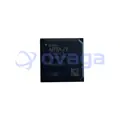
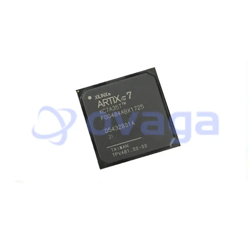
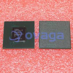
Xilinx XC7A35T-2FGG484I

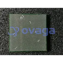
Artix-7 Field Programmable Gate Array (FPGA) IC 250 1843200 33280 484-BBGA


Marques: AMD Xilinx, Inc
Pièce Fabricant #: XC7A35T-2FGG484I
Fiche de données: XC7A35T-2FGG484I Datasheet (PDF)
Colis/Caisse: 484-BBGA
Statut RoHS:
État des stocks: 3505 pièces, nouveau original
type de produit: CI logiques programmables
Warranty: 1 Year Ovaga Warranty - Find Out More
0
1
*Tous les prix sont en USD
| Qté | Prix unitaire | Prix ext |
|---|---|---|
| 1 | $22,592 | $22,592 |
| 10 | $19,416 | $194,160 |
| 60 | $17,978 | $1078,680 |
| 120 | $16,722 | $2006,640 |
In Stock:3505 PCS
XC7A35T-2FGG484I Description générale
The XC7A35T-2FGG484I is a specific member of the Xilinx Artix-7 FPGA (Field-Programmable Gate Array) family. Xilinx provides a range of FPGAs with varying capacities and features to meet different application requirements.
Caractéristiques
FPGA Family: Artix-7 is a family of FPGAs known for offering a balance of low power consumption, high performance, and high logic density. They are suitable for a wide range of applications.
Logic Cells: The "35T" in the part number indicates the number of logic cells in the FPGA. In this case, it has approximately 33,280 logic cells.
Speed Grade: The "-2" in the part number signifies the speed grade of the FPGA. Speed grades represent the maximum frequency at which the FPGA can operate reliably. A lower number is typically faster.
Package Type: The "FGG484" specifies the package type. "FGG" refers to a Fine-Pitch Ball Grid Array (BGA) package with 484 pins.
Industrial Temperature Grade: The "I" in the part number indicates that the device is rated for industrial temperature range.
Configuration: Artix-7 FPGAs support configuration from various sources, including configuration from an external flash memory.
Memory Resources: The FPGA includes on-chip memory resources, such as Block RAM (BRAM) and distributed RAM, which can be used for data storage and processing.
Clock Management: The FPGA provides built-in clock management resources, including PLLs (Phase-Locked Loops) for generating and managing clock signals.
I/O Interfaces: The "484" in the package code indicates the number of I/O pins available in the specific package. These pins can be configured for various purposes, including input, output, and bidirectional communication.Developers use Xilinx Vivado development tools to design, program, and configure these FPGAs for specific applications.
Application
Developers use Xilinx Vivado development tools to design, program, and configure these FPGAs for specific applications.

Caractéristiques
| Paramètre | Valeur | Paramètre | Valeur |
|---|---|---|---|
| Product Name | XC7A35T-2FGG484I | Product Type | Field-Programmable Gate Array (FPGA) |
| Logic Cells | 33,280 | DSP Slices | 90 |
| Block RAM | 1,800 Kbits | Max User I/Os | 200 |
| Operating Frequency | Up to 600 MHz | Programmable Logic Cells | 6-input Look-Up Tables (LUTs) |
| Package | FGG484 | Supply Voltage Range | 1.0V, 1.2V, 1.5V, 1.8V, 2.5V, 3.3V |
| Operating Temperature Range | -40°C to 100°C |
Expédition
| Type d'expédition | Frais d'expédition | Délai de mise en œuvre | |
|---|---|---|---|
 |
DHL | $20.00-$40.00 (0.50 KG) | 2-5 jours |
 |
FedEx | $20.00-$40.00 (0.50 KG) | 2-5 jours |
 |
UPS | $20.00-$40.00 (0.50 KG) | 2-5 jours |
 |
TNT | $20.00-$40.00 (0.50 KG) | 2-5 jours |
 |
EMS | $20.00-$40.00 (0.50 KG) | 2-5 jours |
 |
LA POSTE AÉRIENNE ENREGISTRÉE | $20.00-$40.00 (0.50 KG) | 2-5 jours |
Délai de traitement : les frais d'expédition dépendent des différentes zones et pays.
Paiement
| Modalités de paiement | Frais de main | |
|---|---|---|
 |
Virement bancaire | facturer des frais bancaires de 30,00 $ US. |
 |
Pay Pal | facturer des frais de service de 4,0 %. |
 |
Carte de crédit | facturez des frais de service de 3,5%. |
 |
Western union | charge US.00 banking fee. |
 |
Paiement de Petit Montant | facturer des frais bancaires de 0,00 $ US. |
Garanties
1. Les composants électroniques que vous achetez incluent une garantie de 365 jours, nous garantissons la qualité du produit.
2. Si certains des articles que vous avez reçus ne sont pas de qualité parfaite, nous organiserons de manière responsable votre remboursement ou votre remplacement. Mais les articles doivent rester dans leur état d’origine.
Emballage
-

Étape1 :Produit
-

Étape2 :Emballage sous vide
-

Étape3 :Sac antistatique
-

Étape4 :Emballage individuel
-

Étape5 :Boîtes d'emballage
-

Étape6 :étiquette d'expédition à code-barres


Tous les produits seront emballés dans un sac antistatique. Expédié avec une protection antistatique ESD.
L'étiquette de l'emballage extérieur ESD utilisera les informations de notre société : numéro de pièce, marque et quantité.
Nous inspecterons toutes les marchandises avant expédition, garantirons que tous les produits sont en bon état et que les pièces sont neuves et correspondent à la fiche technique originale.
Une fois que toutes les marchandises sont garanties sans problème après l'emballage, nous les emballerons en toute sécurité et les enverrons par Global Express. Il présente une excellente résistance à la perforation et à la déchirure ainsi qu’une bonne intégrité du joint.


Points de pièce
-
The XC7A35T-2FGG484I chip is a Field-Programmable Gate Array (FPGA) manufactured by Xilinx. It belongs to the Artix-7 family and comes in a 484-ball Fine-Pitch Ball Grid Array (FBGA) package. This chip offers numerous user-programmable logic cells, memory blocks, and I/O pins, making it suitable for various applications requiring programmable logic functionality.
-
Equivalent
Some equivalent products of the XC7A35T-2FGG484I chip include the XC7A35T-1FGG484I and XC7A35T-3FGG484I chips. These alternatives have slightly different specifications, such as lower or higher operating frequency ranges, but offer similar functionality. -
Features
The XC7A35T-2FGG484I is a field-programmable gate array (FPGA) with notable features including 33,280 logic cells, 1,800 Kbits of block RAM, 4,860 slices, 90 DSP slices, and a maximum of 450 MHz clock speed. It offers low power consumption, advanced digital signal processing capabilities, and flexible I/O options for a wide range of applications. -
Pinout
The XC7A35T-2FGG484I is a field-programmable gate array (FPGA) with a pin count of 484. It belongs to the Xilinx Artix-7 family and has a speed grade of -2. The specific pin functions can be found in the datasheet provided by the manufacturer. -
Manufacturer
The manufacturer of the XC7A35T-2FGG484I is Xilinx, Inc. Xilinx is a technology company that specializes in the development and manufacture of programmable logic devices (PLDs) and semiconductor products. They are known for their field-programmable gate arrays (FPGAs) and contribute to a wide range of industries, including automotive, telecommunications, and aerospace. -
Application Field
The XC7A35T-2FGG484I is a field-programmable gate array (FPGA) with a wide range of application areas. It can be used in industries such as automotive, telecommunications, medical devices, aerospace, and defense. With its high logic capacity, low power consumption, and fast performance, this FPGA can handle various complex tasks and computations efficiently. -
Package
The XC7A35T-2FGG484I chip is in a FBGA (Fine-Pitch Ball Grid Array) package type. It has a form factor of 484 pins and its size is 23 x 23 mm.
Fiche de données PDF
Nous fournissons des produits de haute qualité, un service attentionné et une garantie après-vente
-

Nous avons des produits riches, pouvons répondre à vos différents besoins.
-

La quantité minimum de commande commence à partir de 1 pièce.
-

Les frais d'expédition internationaux les plus bas commencent à partir de 0,00 $
-

Garantie de qualité de 365 jours pour tous les produits